Silicon Photonics in Pluggable Optics White Paper
Available Languages
Bias-Free Language
The documentation set for this product strives to use bias-free language. For the purposes of this documentation set, bias-free is defined as language that does not imply discrimination based on age, disability, gender, racial identity, ethnic identity, sexual orientation, socioeconomic status, and intersectionality. Exceptions may be present in the documentation due to language that is hardcoded in the user interfaces of the product software, language used based on RFP documentation, or language that is used by a referenced third-party product. Learn more about how Cisco is using Inclusive Language.
Insatiable demand for network bandwidth is a driving force for new data center technologies. Pushed by growth in video applications, cloud services, gaming, and the number of connected devices, network operators are under continuous pressure to upgrade and expand their network capacity while minimizing spending on new hardware. While much of the focus of hardware upgrades is on the network devices such as routers, switches, and servers, the optical interconnects between these devices are of growing importance in terms of both capital expenditure and operational cost.
The transceiver modules at the ends of the fiber link are a key driver of the performance of the optical interconnect. These are the pluggable optical modules that convert electrical signals to optical signals and back again. They are inserted into the network device and terminate the fiber optic cabling that runs throughout the network’s physical infrastructure. Unlike the ASIC and CPU chips that act as the brains of the network and rely primarily on silicon-based transistors, optical transceivers rely on optical components such as laser diodes, photodiodes, and optical waveguides to manipulate and modulate light to carry information over fiber links.
This white paper focuses specifically on the trend toward building optical devices in silicon. “Silicon photonics,” as it is called, offers the promise of increased integration of optical components and democratization of high-speed optics through high-volume production. Silicon photonics technology has long been of interest in the optical networking industry and in recent years has gained a major foothold in the data center network. This technology is increasingly used for high-speed networks as larger volumes of optical modules are required by data center operators.
Historically, the optics industry has been considered niche, especially compared to the extraordinary scale of the silicon electronics industry. Through decades of effort, the electronics industry has developed mass manufacturing processes based on lithographically patterned silicon wafers. The massive market for electronics has justified economic investment in advanced fabs, material supply chains, automation tools, and design processes for developing and scaling electronics chips.
The optical communications market has been much smaller than the electronics industry, and optics technologies developed along a different technology path, using substrates like gallium arsenide or indium phosphide rather than silicon wafers. Manufacturing techniques tend to be more bespoke in nature and have not benefited from the same economies of scale as electronics.
However, mass production of optics has developed significantly. A focus on manufacturing scalability accelerated during the telecom boom of the late 1990s and continues as optics are deployed more and more within the walls of data centers where copper cabling can’t always support the required reaches at the fastest data rates. Massive deployment of optics has become especially common at cloud and hyperscale data centers. At this point, high-volume manufacturing abilities are critical to meet the demand for data center optics.
This is where silicon photonics becomes interesting. After years of research and development, the technology has reached maturity. In conjunction, the volume driven by the optical transceiver market is large enough for it to leverage the existing massive infrastructure in silicon manufacturing. Piggybacking on the existing supply chains and commercial fabs, silicon photonics allows the production of photonic wafers at large scale. Silicon photonics has matured to the point that it is routinely deployed in real networks and offers true value to end users. In this white paper, we describe the benefits that silicon photonics offers, citing examples from Cisco’s silicon photonics technology base.
Silicon photonics technology integrates the key photonics components and functionality of a high-speed transceiver into a silicon substrate. This enables the use of standard commercial wafer fabrication plants. The technology development for silicon photonics is largely focused on building and qualifying optical components and designs that can be used at the silicon fab to produce photonics systems integrated in a single chip.
An optical transceiver converts electrical signals into optical signals on the transmit side and converts from optical back to electrical on the receive side of a network link. We can highlight the key optical components of a transceiver by following the light as it travels into and out of the device. To receive light, there must be a coupling interface to the silicon, which could be vertical through the top of the chip via grating couplers, or through the side of the silicon with edge coupling. Waveguides steer the light through the chip, and silicon-based photodetectors detect the light and convert the signal to the electrical domain, where it is interpreted by the electronics portion of the device.
On the transmit side, a laser produces the light, which is guided into the chip. That light then needs to be modulated into an information-carrying signal connector. The light is finally coupled out of the chip and into a fiber. From there it can enter fiber cabling external to the transceiver modules via a standard interface.
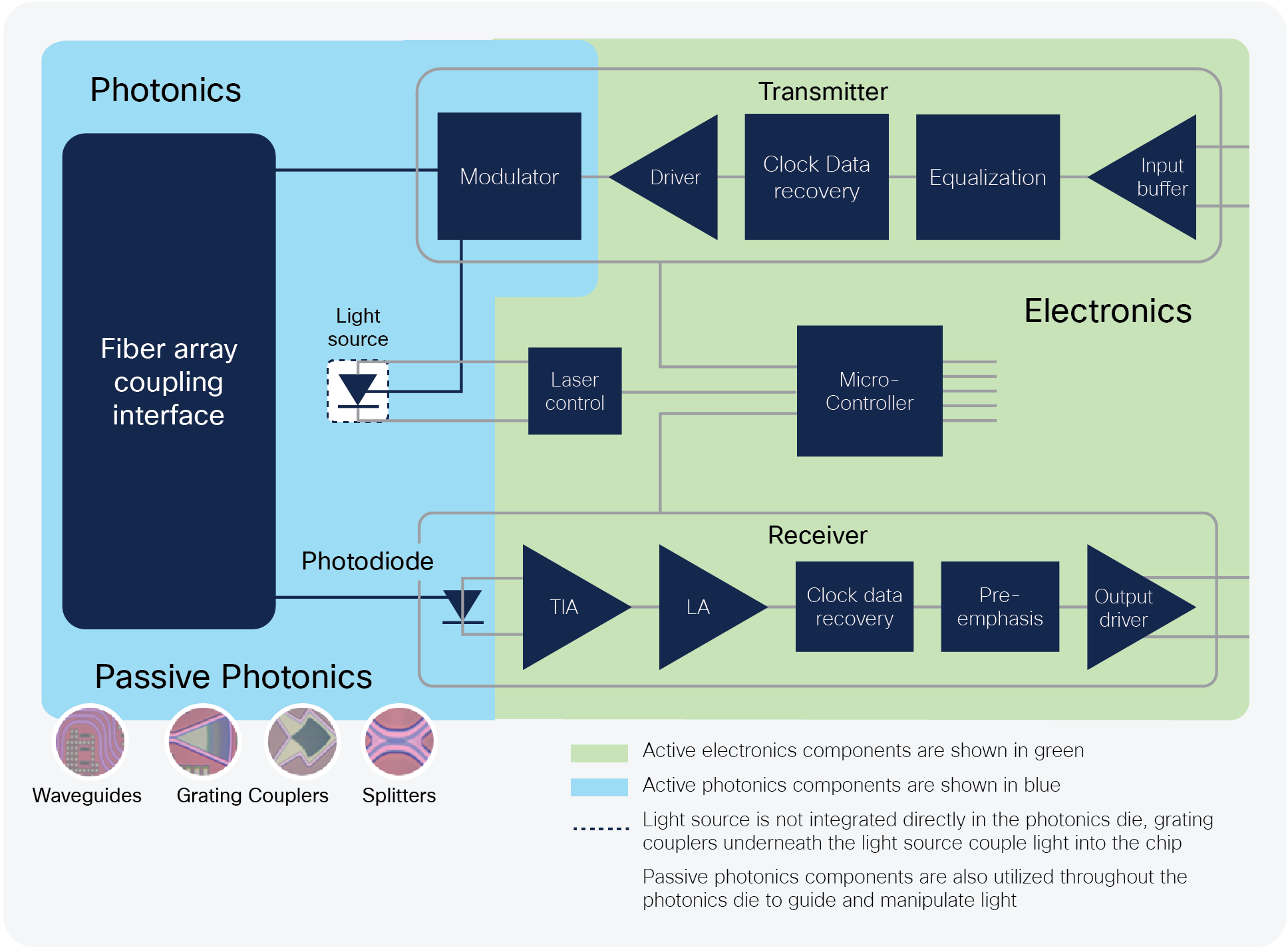
Schematic diagram of an optical transceiver
Historically, photonic devices have been discrete and based on substrates other than silicon, such as indium phosphide or gallium arsenide. In fact, different vendors of the same component may even use different processes. But if each component can be built in the same silicon process, a fully integrated optical chip can be designed and fabricated to leverage the maturity and scale of the CMOS fabrication processes. The photonics die can be closely paired and integrated with an electronics die that handles electrical processing of the signal. An example of a 100-Gbps optical module is shown in the figure below, with the entire transceiver functionality contained in a single chipset. The value of this becomes apparent when optics need to be produced at extremely high scale.
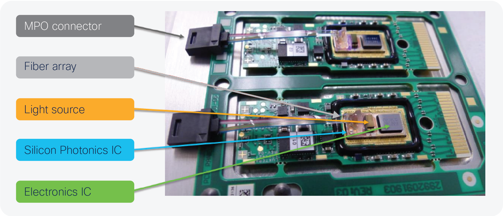
Example of a silicon photonics based 100-Gbps optical module
Manufacturing efficiency and automation
Reduction of manual or bespoke processes helps increase factory output. Silicon photonics enables a highly automated manufacturing flow for optics that involves high-throughput processes and capital equipment. As mentioned previously, the photonics wafer itself is processed in the same commercial semiconductor fabs as electronics wafers. Integration of the optics into a completed module can also leverage standard processes in the electronics industry.
Major assembly and test steps can happen at wafer scale, so the process can be heavily automated and output many units per hour. By leveraging wafer-level capabilities, scaling capacity with this production flow and producing millions of optical transceivers becomes more achievable than ever. And mass production of leading-edge transceivers (data rates from 100G to 400G and beyond) thereby enables mass adoption inside the data center.
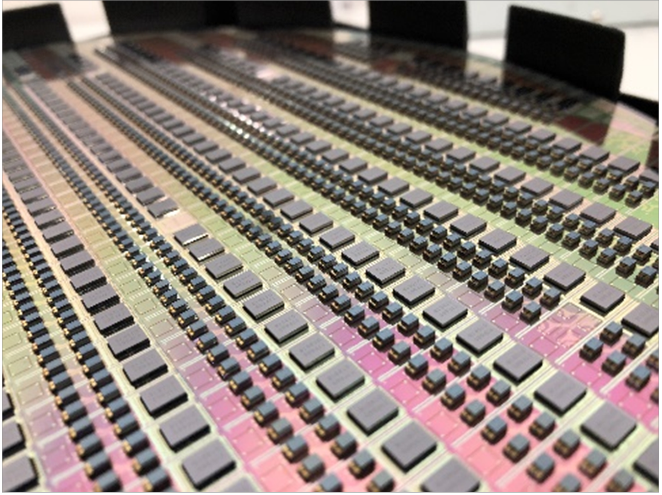
Multiple silicon photonics devices on a single wafer, processed in a commercial semiconductor fab
As optics in general, and silicon photonics more specifically, reach adoption at shorter and shorter reaches, the volume will increase exponentially and reap even more benefits as the overall deployment volumes translate to greater economies of scale. This virtuous cycle, along with the democratization of high-speed data center optics, makes silicon photonics a particularly fascinating area to watch.
Wafer-level testing and module yield
Silicon photonics brings additional benefits along a different axis: reliability and repeatability. The design process for the optics follows a very similar workflow used by a traditional “fabless” electronics company. By defining and compiling the designs of the photonics devices into a photonic device library and design kit, the final design can be fully defined and then etched into silicon by the fab. This results in much less variability in performance than traditional optics that can be affected by later module assembly steps.
The maturity of lithography and wafer etching that is used by the silicon fab allows for well-defined precision and repeatability of the components. This means that statistical models and simulations can help understand and fully determine the performance of the transceiver up front during the design process before material is built. And of course, physical parts can be built and measured to corroborate the accuracy of simulation results. In this way, design-related issues can often be detected and corrected early in the product life cycle.
Once the design is out of fab, there is another unique advantage that comes into play with silicon photonics. It becomes possible to perform wafer-scale testing on the photonics devices before they are diced into individual chips or built up into a module. This results in several important benefits. If there are any failed parts, they can be detected very early on in the build process. The bad die can be mapped and prevented from getting built up with other modules, thus avoiding waste of other components by using only known good die. This has a positive effect on overall yield fallout. This highly testable manufacturing flow and repeatable design performance help to bolster the reliability of the device.
Economies of scale
With silicon chip design, much of the hard work is put in up front in the R&D and design phases of a product. Once the investment is made to design and tape out a chip, silicon can be repeatedly and efficiently stamped out. The up-front, fixed overhead of the design process can be divided over more and more units as volume increases. Over time as optical modules expand throughout the data center market, silicon photonics–based optics will benefit from the ride up the volume curve, and high-speed optics will become more widely available in the market.
Integration with electronics
While the primary application of silicon photonics is in pluggable transceiver modules, there is active development of closer integration with electronics chips and ASICs. One future direction under investigation is to more closely integrate the optics with switch ASICs. Current switch systems have long electrical traces that go from the switch chip to the front panel with ports for pluggable optics. Routing electrical traces from switch to front panel becomes difficult with increasingly fast signaling. Power consumption and cooling challenges are significant obstacles for system designers. If the optics could be integrated more closely with the ASIC, then the length of electrical traces between the switch silicon and the optical I/O is minimized since the signals no longer navigate to a front panel. The formerly high-loss channel is now replaced with a shorter-length, lower-power interface.
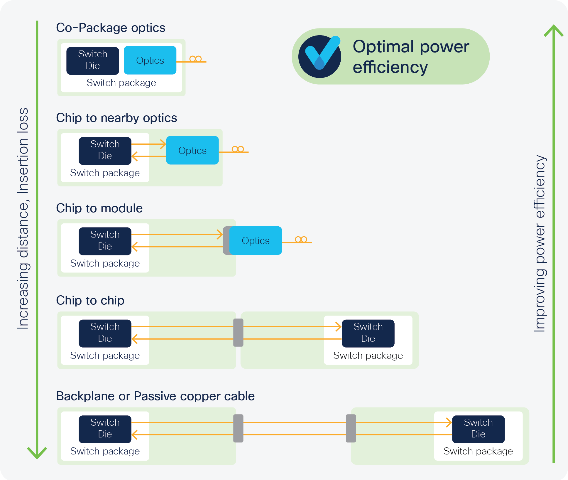
Relation between electrical link length, power efficiency, and type of electrical connectivity
Integrated optics reveals a path forward in a world that requires cost-effective optical I/O, lower system power, and higher bandwidth year after year. The technology components and processes needed to pursue an integrated optics approach will rely heavily on the maturity of silicon photonics. This is a promising long-term future for direct optical I/O. Even further on the horizon, silicon photonics may eventually make high-bandwidth optical interfaces feasible for chip-to-chip interconnects. There will certainly continue to be some exciting technology developments to watch for in this space.
With the benefits of the silicon industry and wafer-scale processes, silicon photonics has defined a new generation of optical transceiver manufacturing. It has already proven to be critical for meeting the demands of the latest network architectures for data centers. As the maximum distances of copper links decline and get replaced by optics, the volume of optical transceiver demand will continue to rise and the benefits of scale will compound itself.