|
CPU
|
Dual AMD™ Turin CPUs, up to 400W TDP each. Each CPU supports 3-link XGMII.
-
Supported CPUs:
-
AMD 9575F 3.3GHz 400W 64C/256MB Cache DDR5 6000MT/s (CAI-CPU-A9575F)
-
AMD 9475F 3.65GHz 400W 48C/256MB Cache DDR5 6000MT/s (CAI-CPU-A9475F)
-
AMD 9375F 3.85GHz 320W 32C/256MB Cache DDR5 6000MT/s (CAI-CPU-A9375F)
-
AMD 9655 2.6GHz 400W 96C/384MB Cache DDR5 6000MT/s (CAI-CPU-A9655)
-
AMD 9555 3.2GHz 360W 64C/256MB Cache DDR5 6000MT/s (CAI-CPU-A9555)
-
AMD 9455 3.15GHz 300W 48C/256MB Cache DDR5 6000MT/s (CAI-CPU-A9455)
-
AMD 9355 3.55GHz 280W 32C/256MB Cache DDR5 6000MT/s (CAI-CPU-A9355)
|
|
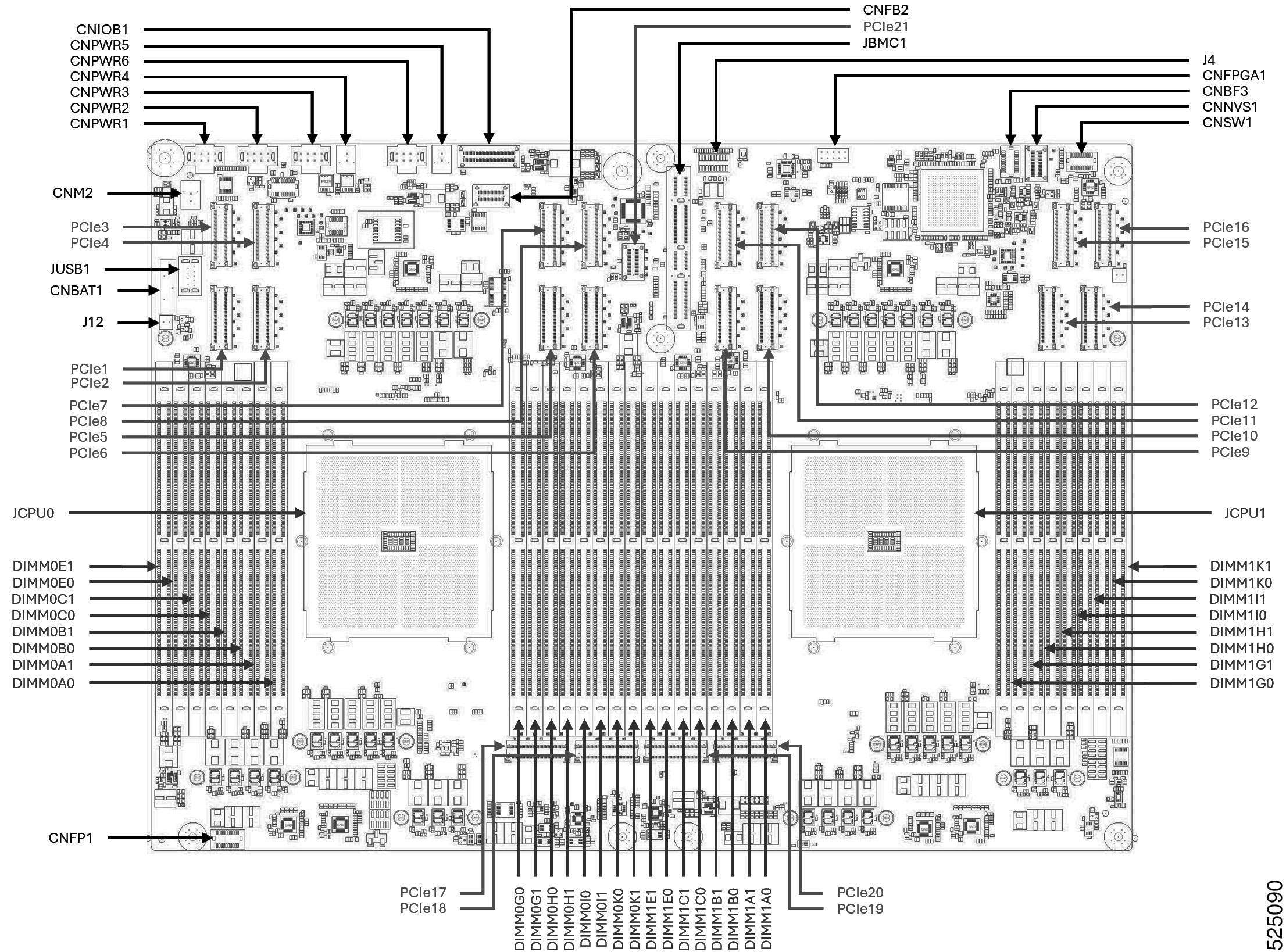
System Memory
|
Up to 32 DDR5 DIMMs:
-
32GB DDR5-6400 RDIMM 1Rx4 (16Gb) (CAI-MRx32G1RE5)
-
64GB DDR5-6400 RDIMM 2Rx4 (16Gb) (CAI-MRx64G2RE5)
-
96GB DDR5-6400 RDIMM 2Rx4 (24Gb) (CAI-MRx96G2RF5)
-
128GB DDR5-6400 RDIMM 2Rx4 (32Gb) (CAI-MR128G2RG5)
-
256GB DDR5-6400 RDIMM 4Rx4 (32Gb) (CAI-MR256G4RG5)
|
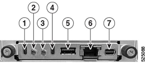
| System Control |
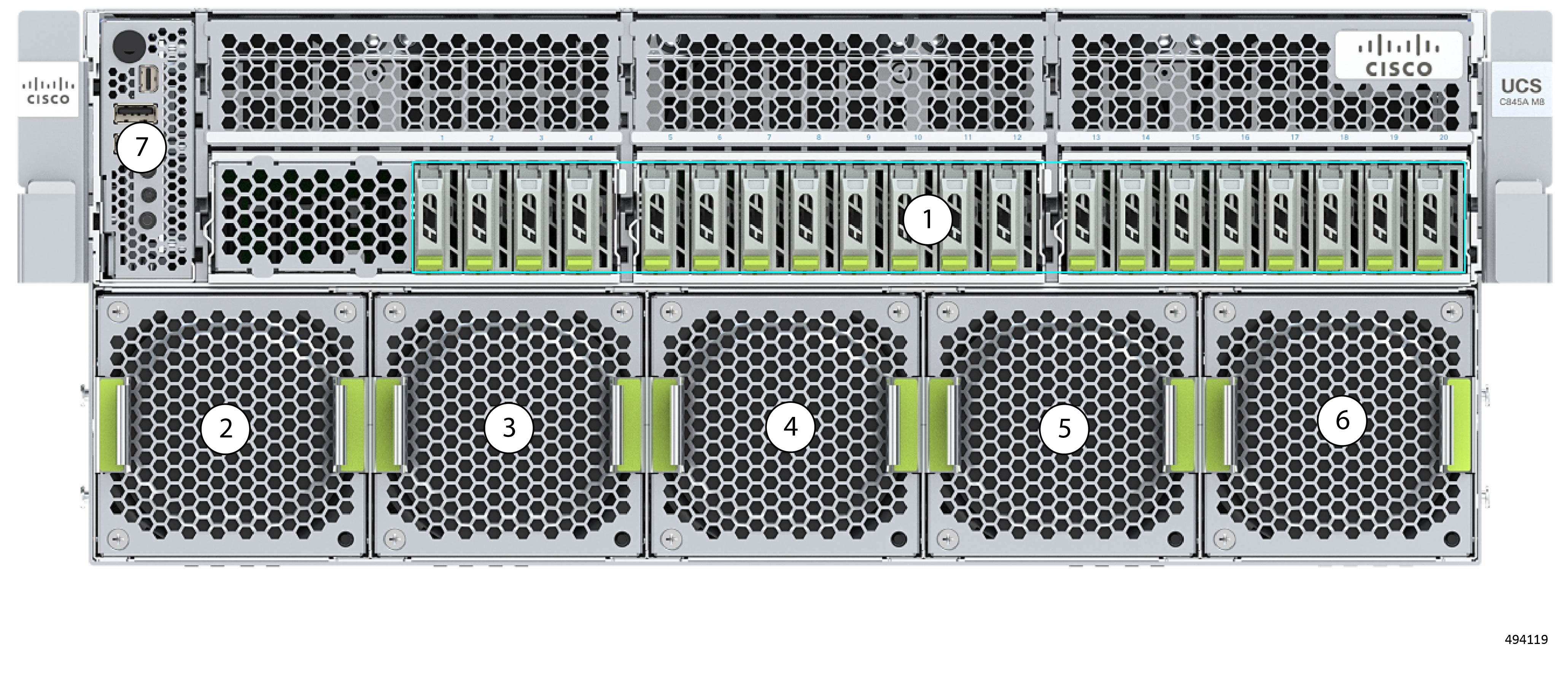
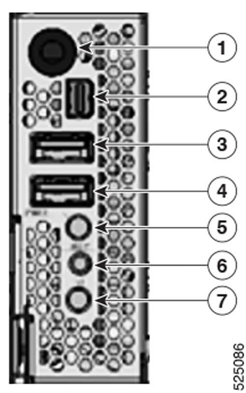
Dedicated RJ-45 Ethernet port which provides physical access to the server’s baseboard management controller (BMC)
|
|
GPU
|
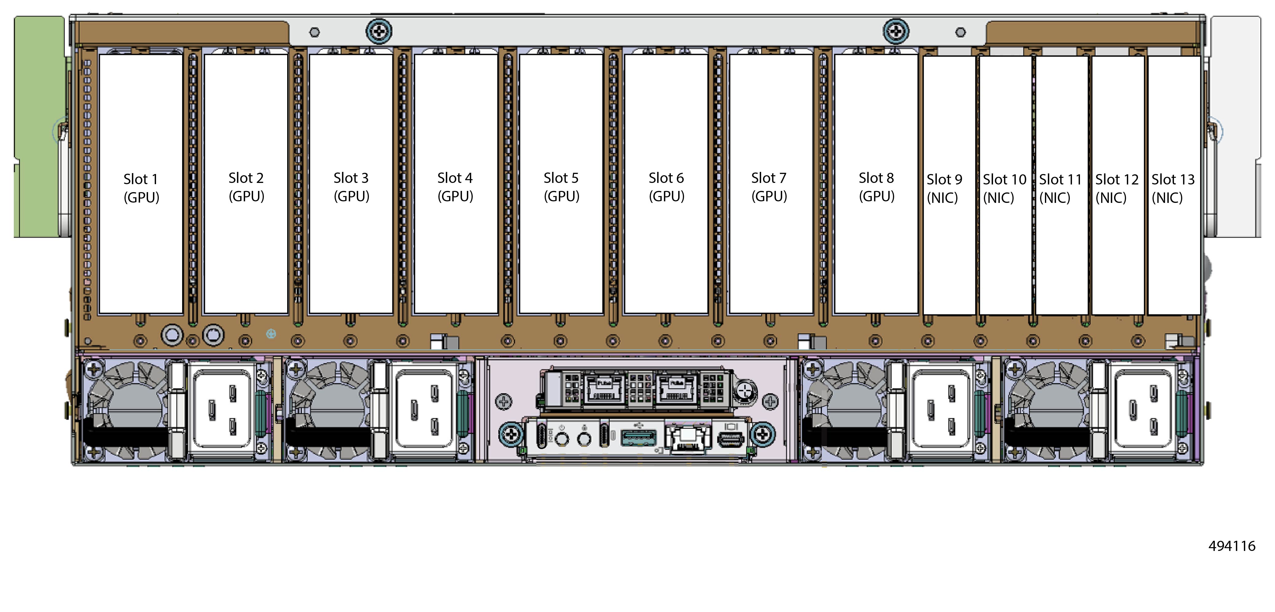
Two, four, six, or eight of the following PCIe GPUs:
-
AMD™ Instinct MI210 GPU, 300W, 64GB, FHFL, 2-slot (CAI-GPU-MI210). This GPU supports AMD's 2-Way and 4-Way GPU interconnect.
-
NVIDIA™ RTX Pro 6000 GPU, 600W, 96GB, FHFL, 2-slot (CAI-GPU-RTXP6000)
-
NVIDIA RTX Pro 6000D GPU, 600W, 84GB, FHFL, 2-slot (CAI-GPU-RTXP6000D)
-
NVIDIA L40S: 350W, 48GB, 2-slot FHFL GPU (CAI-GPU-L40S)
-
NVIDIA OEM H200-NVL GPU 600W, 141GB, 2-slot FHFL (CAI-GPU-H200-NVL). This GPU supports NVIDIA's 2-Way and 4-Way NVLink GPU
interconnect.
-
NVIDIA RTX Pro 4500 GPU, 165W, 32GB, FHFL, 1-slot (CAI-GPU-RTXP4500)
|
Note
|
If your system will use this GPU, or another single-width GPU, make sure to obtain a perforated filler panel by ordering (UCSC-PCIE-FH).
The number of perforated filler panels you will need equals (16 - x) where x is the number of single-width GPUs.
|
|
|
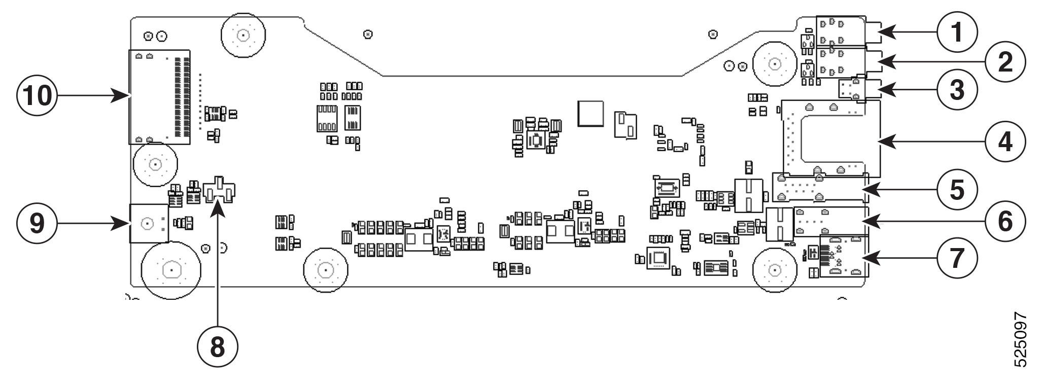
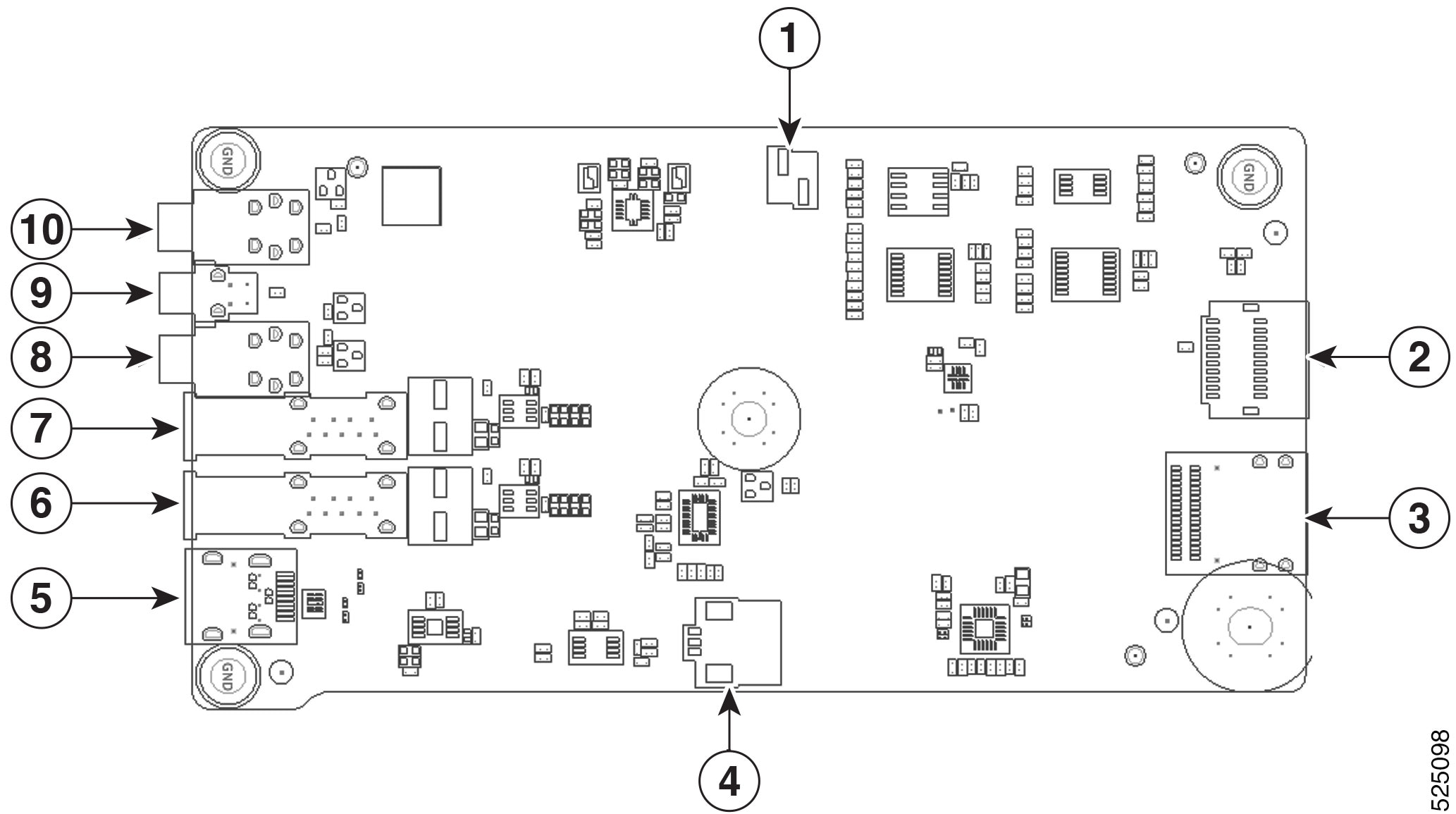
LAN
|
One OCP 3.0 SFF PCIe Gen5 x8 NIC (CPU0) with two 10GbE RJ-45 Ethernet
|
|
Management
|
Supported through the DC-SCM card, which features an AST2600 BMC
Security is offered through a version 3.0 trusted platform module (TPM).
One OCP 3.0 10GBaseT module offers server host management.
|
|
Storage
|
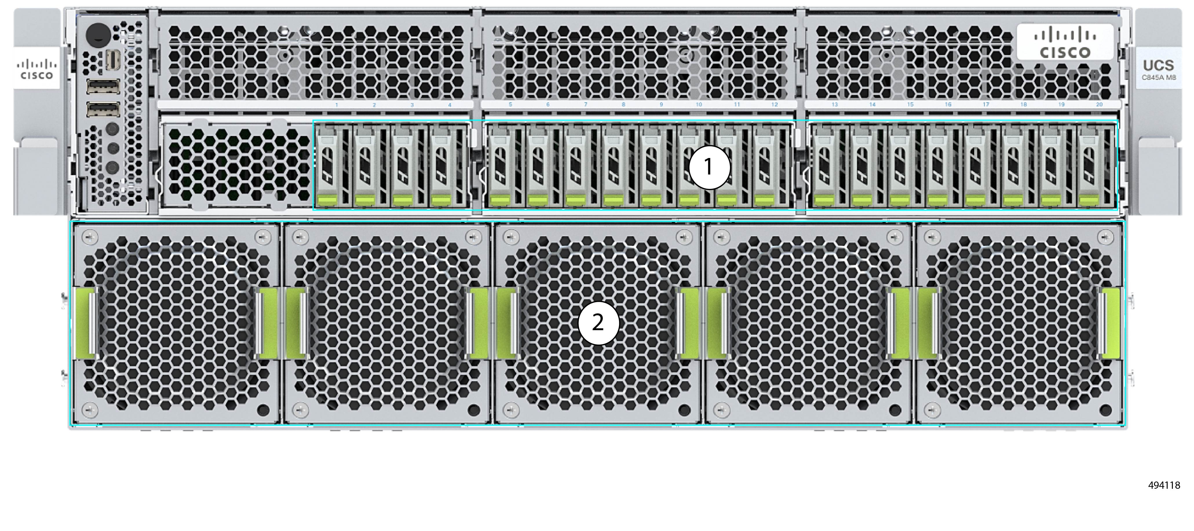
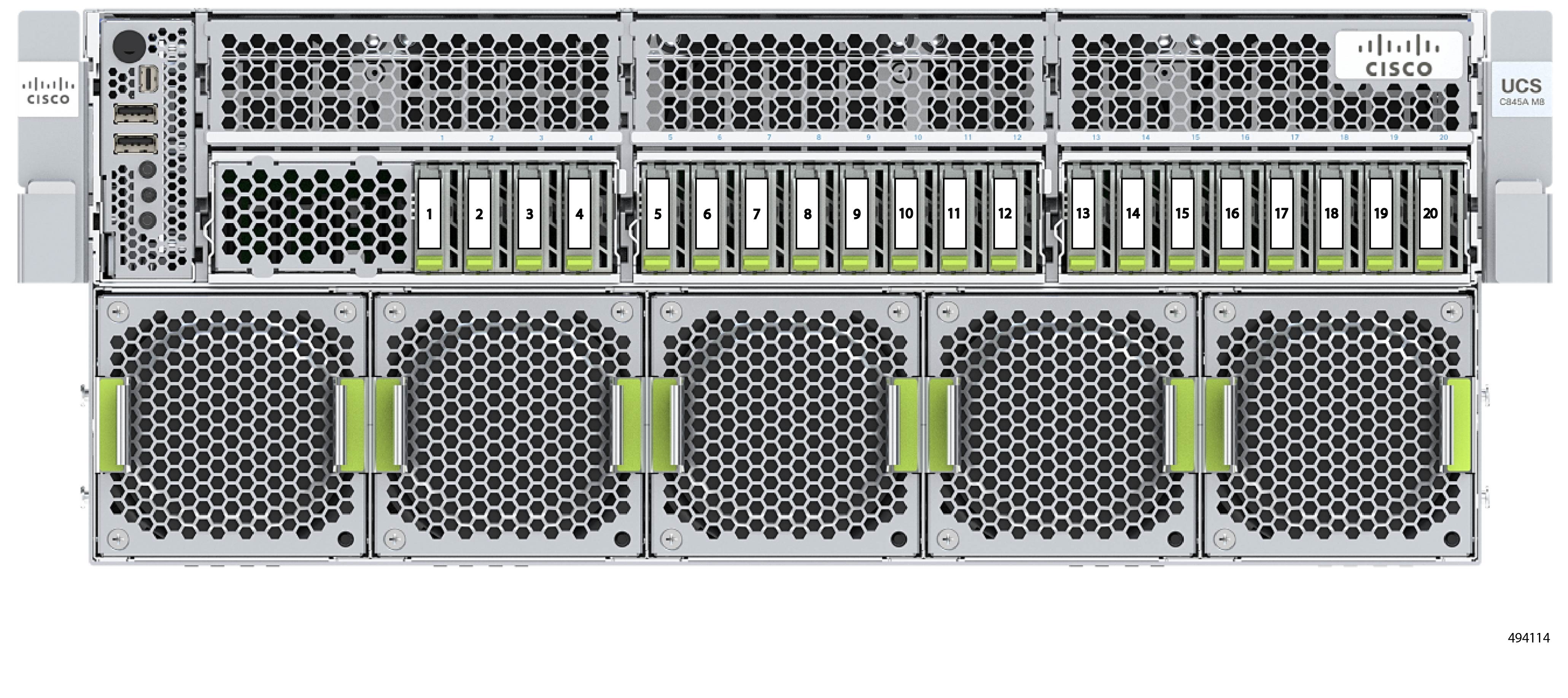
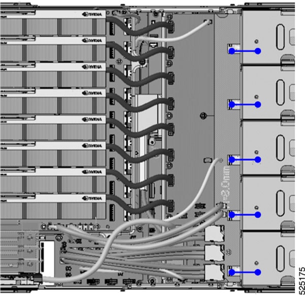
Up to 20 E1.S NVMe PCIe Gen5 SSDs.
-
1.9TB E1.S 15mm Kioxia™ XD7P Hg Perf Med End Gen4 1X NVMe (CAI-NVES1T9K1V)
-
3.8TB E1.S 15mm Kioxia XD7P Hg Perf Med End Gen4 1X NVMe (CAI-NVES3T8K1V)
-
7.6TB E1.S 15mm Kioxia XD7P Hg Perf Med End Gen4 1X NVMe (CAI-NVES7T6K1V)
-
1.9TB E1.S 15mm Kioxia XD8 Hg Perf Med End Gen5 1X NVMe (CAI-NVES1T9K2V)
-
3.8TB E1.S 15mm Kioxia XD8 Hg Perf Med End Gen5 1X NVMe (CAI-NVES3T8K2V)
-
7.6TB E1.S 15mm Kioxia XD8 Hg Perf Med End Gen5 1X NVMe (CAI-NVES7T6K2V)
-
1.9TB E1.S 15mm Sandisk SN861 Hg Perf Med End Gen5 1X NVMe (CAI-NVES1T9D1V)
-
3.8TB E1.S 15mm Sandisk SN861 Hg Perf Med End Gen5 1X NVMe (CAI-NVES3T8D1V)
-
7.6TB E1.S 15mm Sandisk SN861 Hg Perf Med End Gen5 1X NVMe (CAI-NVES7T6D1V)
-
15.3TB E1.S 15mm Sandisk SN861 Hg Perf Med End Gen5 1X NVMe (CAI-NVES15T3D1V)
Boot Drives: A Cisco Boot-Optimized RAID controller with two M.2 SATA boot drives is also supported in either few the following
configurations.
|
|
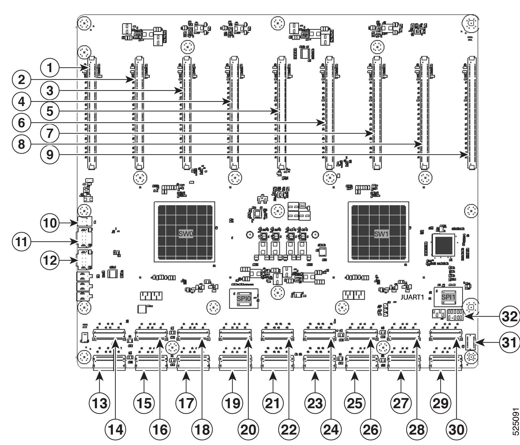
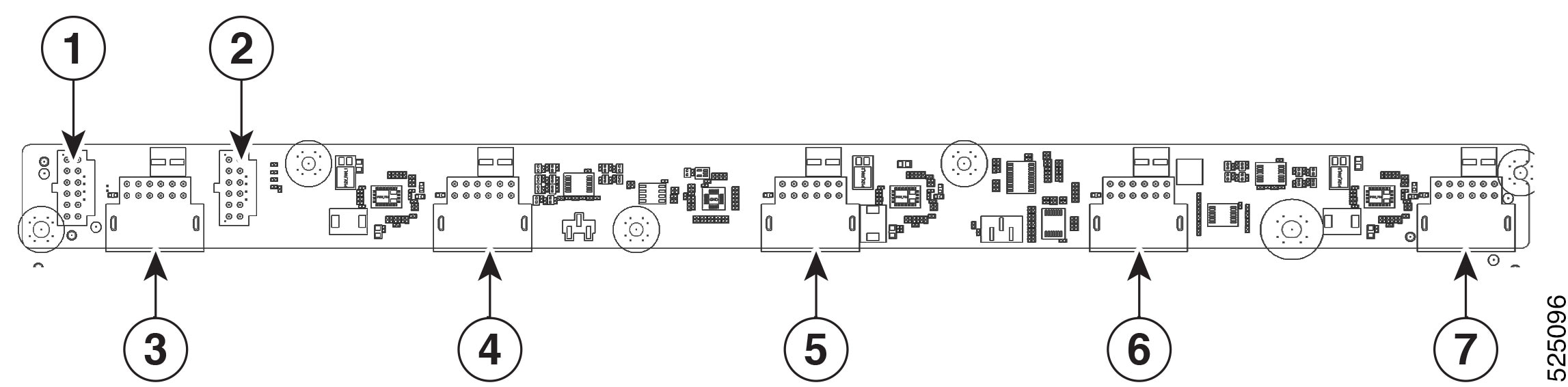
Expansion Slot
|
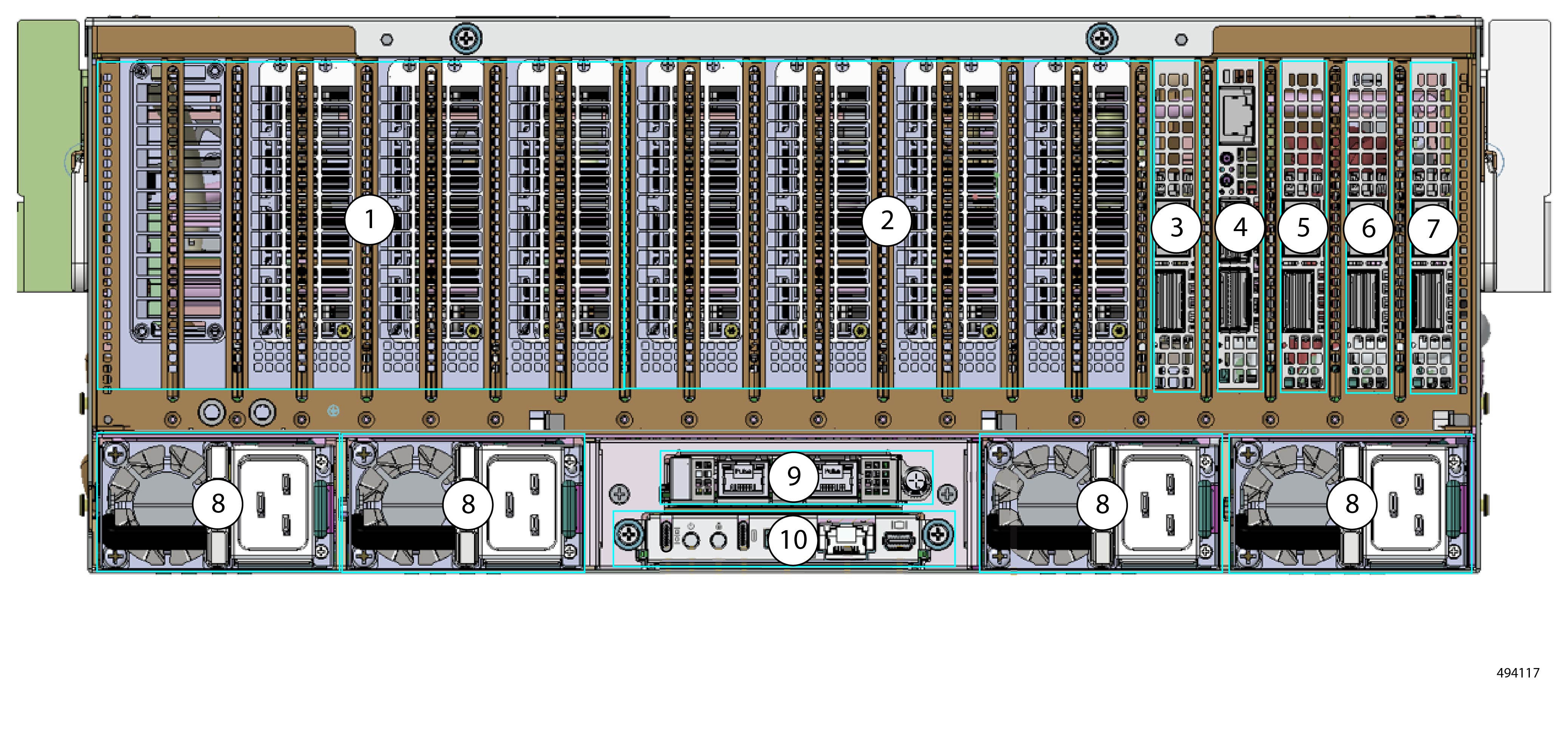
Five FHHL PCIe Gen5 x16 slots
One OCP 3.0 slot
|
| Networking |
Five PCIe x16 full height, half length (FHHL) slots for single-slot NICS or data processing units (DPUs)
For north-south traffic:
-
NVIDIA MCX755106AS-HEAT 2x200GbE QSFP112 Gen5x16, PCIe VPI NIC (CAI-P-N7D200GFO)
-
NVIDIA BF-3 B3220 DPU 2x200G QSFP112, Crypto Disabled (CAI-P-N3220)
-
Intel X710-DA2 (2x10GbE) (RJ45 OCP 3.0) (CAI-O-ID10GC)
-
NVIDIA BF-3 B3220 DPU 2x200G Crypto enabled (CAI-P-NC3220)
-
NVIDIA OEM CX713104AS-ADAT: 4x25GbE SFP56 Gen4x16, PCIe NIC (CAI-P-N7Q25GFO)
For east-west traffic:
-
NVIDIA OEM BlueField-3 B3140H SuperNIC 1x400G Crypto Disabled (CAI-P-N3140H)
-
NVIDIA OEM MCX715105AS-WEAT 1x400GbE QSFP112 PCIe Gen5 NIC, Crypto Disabled (CAI-P-N7S400GFO)
-
NVIDIA BF-3 B3140H SuperNIC 1x400G Crypto enabled (CAI-P-NC3140H)
-
NVIDIA OEM CX713104AS-ADAT: 4x25GbE SFP56 Gen4x16, PCIe NIC (CAI-P-N7Q25GFO)
|
|
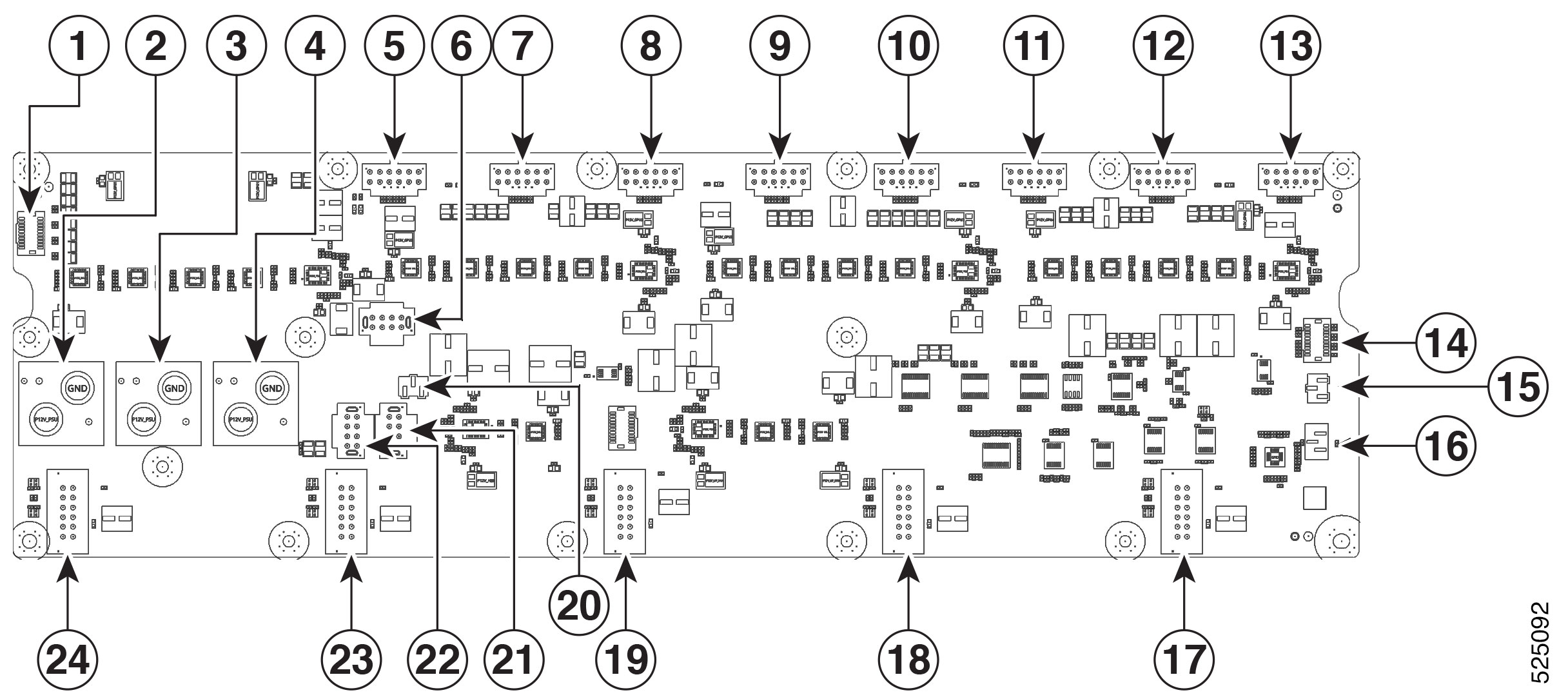
System Cooling
|
Five individual 80 mm fans
|
|
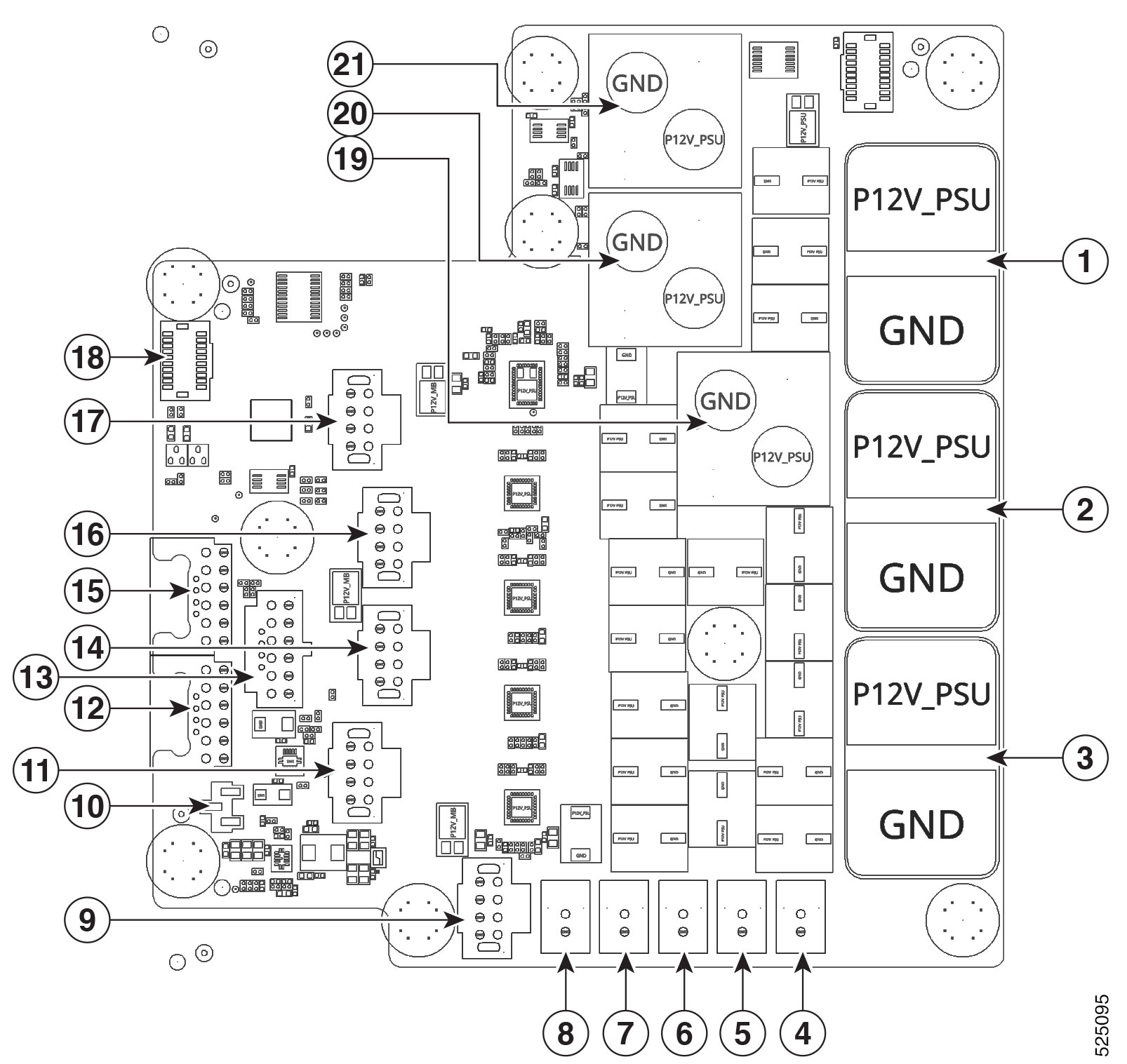
Power
|
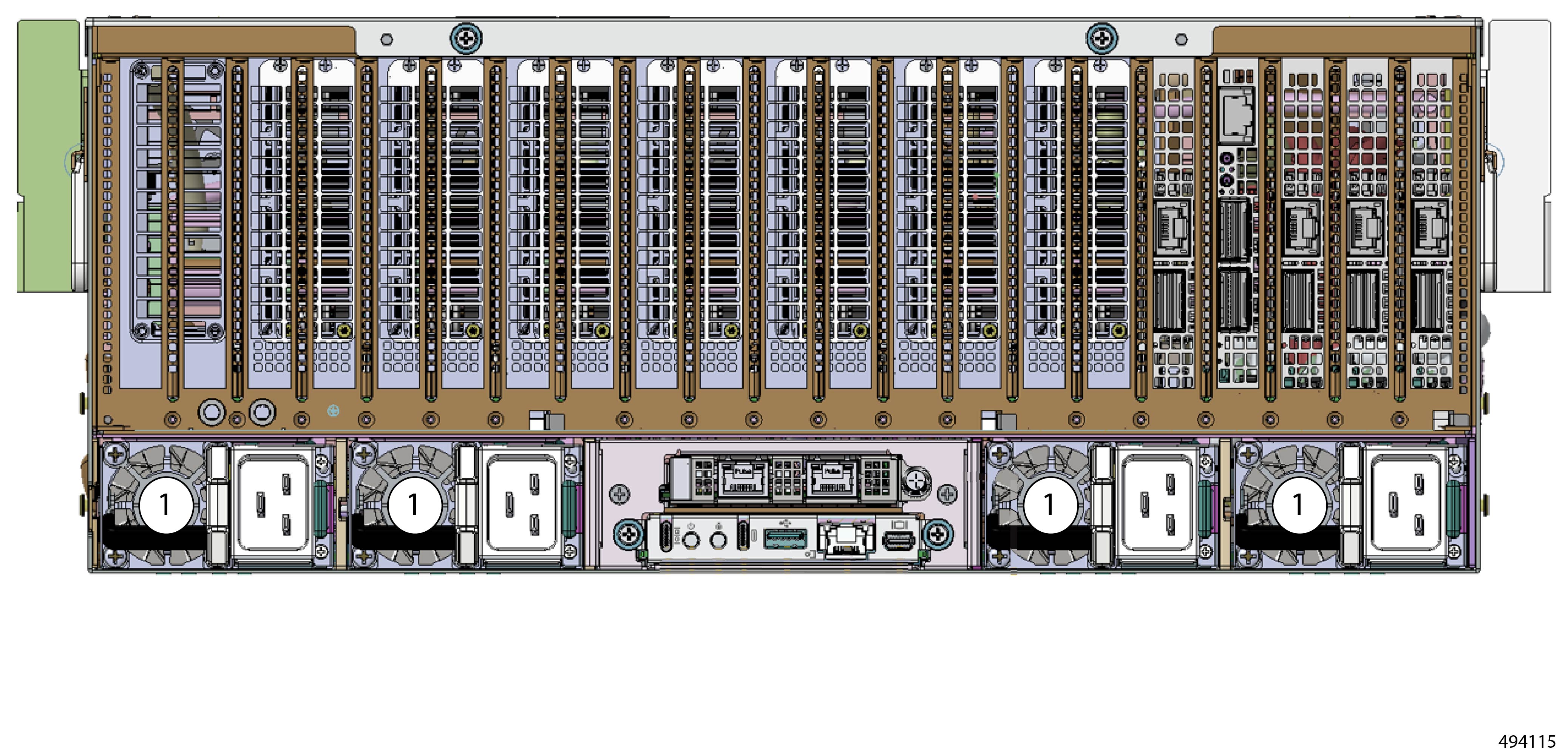
Up to four 3.2KW MCRPS hot-swappable PSUs with N+1 redundancy
|
|
System BIOS
|
AMI™ BIOS
|
|
System Software
|
AMD ROCm™ Software Ubuntu / Red Hat Enterprise Linux (operating system)
|


 Feedback