Installing the Cisco ONS 15216-MD-48-ODD, 15216-MD-48-ODDE, 15216-MD-48-EVENE, and 15216-MD-48-EVEN Mux/Demux Exposed Faceplate Patch Panels
This document explains how to install and operate the Cisco ONS 15216-MD-48-ODD, 15216-MD-48-ODDE, 15216-MD-48-EVENE, and 15216-MD-48-EVEN Mux/Demux Exposed Faceplate patch panels.
Overview of the ONS 15216-MD-48-ODD, ONS 15216-MD-48-ODDE, and ONS 15216-MD-48-EVENE and ONS 15216-MD-48-EVEN Mux/Demux Patch Panels
The ONS 15216-MD-48-ODD=/15216-MD-48-ODDE= and ONS 15216-MD-48-EVEN=/15216-MD-48-EVENE= units are the Cisco ONS 15216 exposed faceplate multiplexer/demultiplexer patch panels of 48-channels spaced at 100 GHz on the odd or even ITU grid respectively. The difference between the ONS 15216-MD-48-ODD/15216-MD-48-ODDE and ONS 15216-MD-48-EVEN/15216-MD-48-EVENE patch panel is the operating 100 GHz ITU grid.
The ONS 15216-MD-48-ODD/15216-MD-48-ODDE or ONS 15216-MD-48-EVEN/15216-MD-48-EVENE patch panel enables 48-channels of ITU wavelengths to be placed or removed from a single fiber. For C-band channel wavelength plan for the odd and even patch panels, see "Channel Wavelength Allocation".
 Note |
Unless otherwise specified, "ONS 15216-MD", , or “Patch Panel” refers to both odd and even patch panels. The odd and even patch panels mentioned in this document refers to the Cisco ONS 15216-MD-48-ODD/15216-MD-48-ODDE and Cisco ONS 15216-MD-48-EVEN/15216-MD-48-EVENE patch panels. |
The patch panel can combine 48-channels of ITU wavelengths spaced at 100 GHz to a denser DWDM signal and separate the combined signal to 48-channels of ITU wavelengths spaced at 100 GHz. To increase the network capacity, the patch panel is plugged with a Cisco ONS 15216 50/100 GHz Interleaver and Deinterleaver module (15216-MD-48-CM) for ONS 15216-MD-48-ODD= and ONS 15216-MD-48-EVEN= units. To increase the network capacity, the patch panel is plugged with a Cisco ONS 15216 50/100 GHz Coupler and Splitter module (15216-MD-48-CME) for ONS 15216-MD-48-ODDE= and ONS 15216-MD-48-EVENE= units. The patch panel can then be used along with another patch panel of a different grid (odd or even).
The interleaver or coupler module combines the signals from the 15216-MD-48-ODD/15216-MD-48-ODDE and 15216-MD-48-EVEN/15216-MD-48-EVENE patch panels spaced at 100 GHz to a denser DWDM signal spaced at 50 GHz and the deinterleaver or splitter module splits the combined signal (96 channel signal) to the 15216-MD-48-ODD/15216-MD-48-ODDE and 15216-MD-48-EVEN/15216-MD-48-EVENE patch panels in the opposite direction.
Note |
|
Features
The Cisco ONS 15216 MD 48-channel mux/demux patch panel provides signal multiplexing and demultiplexing in 100 GHz channel-spacing DWDM systems. It is optically and electrically passive and requires no temperature control. It uses fused fiber coupler and birefringent crystal technologies. The ultra-low dispersion of the patch panel coupled with the wide bandwidth reduces dispersion accumulation and bandwidth narrowing, making the patch panel ideal for multi-OADM metro-ring or mesh-based architectures.
-
Low dispersion
-
Low insertion loss
-
High channel isolation
-
Wide clear bandwidth
-
Full C-band coverage
-
Multiplex and demultiplex 48-channels
-
Athermal design
The patch panel works with 50 GHz and 100 GHz WXC cards. However, when used with a 50 GHz card, the patch panel should be used with a pluggable interleaver and deinterleaver module along with another patch panel of a different grid (odd or even).
-
Point-to-point network
-
Hub node for an open-ring network
-
Multiplex add/drop for multi-degree ROADM
Functional Description
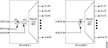
The mux module combines signals from Chi-RX ports (48-channels) into the aggregated COM-TX port. An integrated tap-coupler combines the aggregated signals with the additional external sources injected at AUX-MUX port and splits 1% of the aggregated signals towards the MON-MUX port that is used for monitoring purpose.
The demux module separates the aggregated signals into individual Chi-TX ports. An integrated tap-coupler splits 1% of the aggregated signals coming from the COM-RX port towards MON-DMX port that is used for monitoring.
Channel Wavelength Allocation
The following table describes the C-band channel wavelength allocation plan for the odd and even patch panels.
| Channel Wavelength | Channel Wavelength | ||||
|---|---|---|---|---|---|
| 15216-MD-48-ODD/15216-MD-48-ODDE | 15216-MD-48-EVEN/15216-MD-48-EVENE | ||||
| Channel Label | Frequency (THz) | Wavelength (nm) | Channel Label | Frequency (THz) | Wavelength (nm) |
| 1 | 196.1 | 1528.77 | 1 | 196.05 | 1529.16 |
| 2 | 196.0 | 1529.55 | 2 | 195.95 | 1529.94 |
| 3 | 195.9 | 1530.33 | 3 | 195.85 | 1530.72 |
| 4 | 195.8 | 1531.12 | 4 | 195.75 | 1531.51 |
| 5 | 195.7 | 1531.90 | 5 | 195.65 | 1532.29 |
| 6 | 195.6 | 1532.68 | 6 | 195.55 | 1533.07 |
| 7 | 195.5 | 1533.47 | 7 | 195.45 | 1533.86 |
| 8 | 195.4 | 1534.25 | 8 | 195.35 | 1534.64 |
| 9 | 195.3 | 1535.04 | 9 | 195.25 | 1535.43 |
| 10 | 195.2 | 1535.82 | 10 | 195.15 | 1536.22 |
| 11 | 195.1 | 1536.61 | 11 | 195.05 | 1537.00 |
| 12 | 195 | 1537.40 | 12 | 194.95 | 1537.79 |
| 13 | 194.9 | 1538.19 | 13 | 194.85 | 1538.58 |
| 14 | 194.8 | 1538.98 | 14 | 194.75 | 1539.37 |
| 15 | 194.7 | 1539.77 | 15 | 194.65 | 1540.16 |
| 16 | 194.6 | 1540.56 | 16 | 194.55 | 1540.95 |
| 17 | 194.5 | 1541.35 | 17 | 194.45 | 1541.75 |
| 18 | 194.4 | 1542.14 | 18 | 194.35 | 1542.54 |
| 19 | 194.3 | 1542.94 | 19 | 194.25 | 1543.33 |
| 20 | 194.2 | 1543.73 | 20 | 194.15 | 1544.13 |
| 21 | 194.1 | 1544.53 | 21 | 194.05 | 1544.92 |
| 22 | 194 | 1545.32 | 22 | 193.95 | 1545.72 |
| 23 | 193.9 | 1546.12 | 23 | 193.85 | 1546.52 |
| 24 | 193.8 | 1546.92 | 24 | 193.75 | 1547.32 |
| 25 | 193.7 | 1547.72 | 25 | 193.65 | 1548.11 |
| 26 | 193.6 | 1548.51 | 26 | 193.55 | 1548.91 |
| 27 | 193.5 | 1549.32 | 27 | 193.45 | 1549.72 |
| 28 | 193.4 | 1550.12 | 28 | 193.35 | 1550.52 |
| 29 | 193.3 | 1550.92 | 29 | 193.25 | 1551.32 |
| 30 | 193.2 | 1551.72 | 30 | 193.15 | 1552.12 |
| 31 | 193.1 | 1552.52 | 31 | 193.05 | 1552.93 |
| 32 | 193 | 1553.33 | 32 | 192.95 | 1553.73 |
| 33 | 192.9 | 1554.13 | 33 | 192.85 | 1554.54 |
| 34 | 192.8 | 1554.94 | 34 | 192.75 | 1555.34 |
| 35 | 192.7 | 1555.75 | 35 | 192.65 | 1556.15 |
| 36 | 192.6 | 1556.55 | 36 | 192.55 | 1556.96 |
| 37 | 192.5 | 1557.36 | 37 | 192.45 | 1557.77 |
| 38 | 192.4 | 1558.17 | 38 | 192.35 | 1558.58 |
| 39 | 192.3 | 1558.98 | 39 | 192.25 | 1559.39 |
| 40 | 192.2 | 1559.79 | 40 | 192.15 | 1560.20 |
| 41 | 192.1 | 1560.61 | 41 | 192.05 | 1561.01 |
| 42 | 192 | 1561.42 | 42 | 191.95 | 1561.83 |
| 43 | 191.9 | 1562.23 | 43 | 191.85 | 1562.64 |
| 44 | 191.8 | 1563.05 | 44 | 191.75 | 1563.45 |
| 45 | 191.7 | 1563.86 | 45 | 191.65 | 1564.27 |
| 46 | 191.6 | 1564.68 | 46 | 191.55 | 1565.09 |
| 47 | 191.5 | 1565.50 | 47 | 191.45 | 1565.90 |
| 48 | 191.4 | 1566.31 | 48 | 191.35 | 1566.72 |
Port Label Description
The channel identification labels provide port identification. The Channel ID label is placed on the front panel. The below table lists the connection ports, description, and the type of connectors used for each port. All ports are on the front faceplate, which is equipped with optical LC adapters and one USB Type A receptacle connector.
| Port Label | Description | Type of Connector |
|---|---|---|
| COM-RX | Common input | LC-UPC II |
| COM-TX | Common output | LC-UPC II |
| Chi_RX | Channel input | LC-UPC II |
| Chi_TX | Channel output | LC-UPC II |
| MON-DMX | Monitor port-demux section | LC-UPC II |
| MON-MUX | Monitor port-mux section | LC-UPC II |
| AUX-MUX | Auxiliary input-mux section | LC-UPC II |
| INV | USB inventory port | USB Type A receptacle connector |
Performance Monitoring
The patch panel uses Optical Test Access Port (TAP) devices to enable passive access and monitoring in the fiber-optic network. TAPs enable network-based intrusion detection system sensors to operate efficiently without interruption. They send traffic data to a monitoring device by splitting the network signal, without introducing delay or changing the content or structure of the information contained in the packets. An optical spectrum analyzer (OSA) ) or power meter (PM) can be used for optical power monitoring and optical analysis.
The following table shows the manufacturer-specified TAP split ratios for the TAP coupler optical power in the patch panel. The split ratio denotes the ratio of the TAP input signal to the output signal.
| Parameter | Condition | Minimum | Maximum | Units |
|---|---|---|---|---|
| Monitor Attenuation MUX | Attenuation = IL1 - IL2, where IL1 = Ch1-RX to MON-MUX Insertion Loss and IL2 = Ch1-RX to COM-TX Insertion Loss. | 18 | 22 | dB |
| Monitor Attenuation DEMUX | COM-RX to MON-DMX Insertion Loss | 18 | 22 | dB |
Safety Information
Before you install, operate, or service this product, you must read the Regulatory Compliance and Safety Information for Cisco Optical Transport Products document for important safety information and warning translations.
This product is compliant with the GR 1089, UL60950 /CSA 22.2 No. 60950-00, and IEC 60950 standards.
Laser Radiation Emission Restrictions
The Class 1M Laser safety and warning label is affixed to this product and indicates that the product should never be used or installed in an optical network with emissions higher than Class 1M.
 Warning |
Class 1M laser radiation when open. Do not view directly with optical instruments. Statement 281 |
Warning |
Invisible laser radiation may be emitted from disconnected fibers or connectors. Do not stare into beams or view directly with optical instruments. Statement 1051 |
Electrical Safety
This product is optically and electrically passive and requires no electrical connections. No electrostatic discharge (ESD) or other electrical safety considerations apply.
Mounting Brackets and Rack Equipment
-
19-inch (482.6-mm) or 23-inch (584.2-mm) reversible (two-way) mounting brackets that can be rotated to fit either rack size. These reversible brackets are used for EIA and IEC standard racks.
-
ETSI brackets that are used for 600 mm x 600 mm or 600 mm x 300 mm ETSI racks.
Note |
The patch panel is shipped with the mounting brackets in the 19-inch (482.6-mm) position. |
-
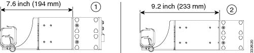
4.2, 4.9, 7.6, or 9.2 inches from the front of the EIA standard racks fixing plane (or)
-
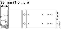
39 mm from the front of the ETSI standard racks fixing plane (or)
-
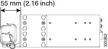
55 mm from the front of the IEC standard racks fixing plane
Diagram 1 in the following figure shows 4.2 inch recess location for EIA standard racks.
Diagram 2 in the following figure shows 4.9 inch recess location for EIA standard racks.
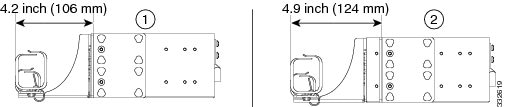
Diagram 1 in the following figure shows 7.6 inch recess location for EIA standard racks.
Diagram 2 in the following figure shows 9.2 inch recess location for EIA standard racks.
The following figure shows 39 mm recess location for ETSI standard racks.
The following figure shows 55 mm recess location for IEC standard racks.
Unpacking and Verifying the ONS 15216 MD Odd and Even Patch Panels
SUMMARY STEPS
- Unpack and inspect the module. The package should include these components:
- Compare the equipment received with the packing slip and the equipment list that the customer service representative provided. If there are any discrepancies, notify the Customer Service Center.
- Check for external damage. Visually check all components and immediately report any shipping damage to your customer service representative. Have this information ready:
DETAILED STEPS
| Step 1 |
Unpack and inspect the module. The package should include these components:
|
||
| Step 2 |
Compare the equipment received with the packing slip and the equipment list that the customer service representative provided. If there are any discrepancies, notify the Customer Service Center. |
||
| Step 3 |
Check for external damage. Visually check all components and immediately report any shipping damage to your customer service representative. Have this information ready:
|
Installing the Patch Panels
 Caution |
Use only the fastening hardware provided with the ONS 15216 MD odd and even patch panel to prevent loosening, deterioration, and electromechanical corrosion of the hardware and joined material. |
Caution |
When mounting the ONS 15216 MD odd and even patch panel in a frame with a nonconductive coating (such as paint, lacquer, or enamel) use either the thread-forming screws provided with the ONS 15216 MD patch panel shipping kit or remove the coating from the threads to ensure electrical continuity. |
SUMMARY STEPS
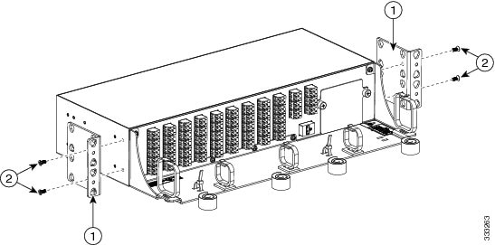
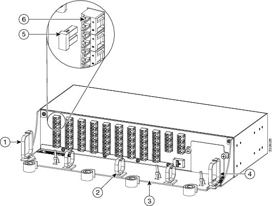
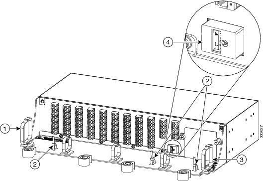
- Mount the brackets on the patch panel (see the following figure):
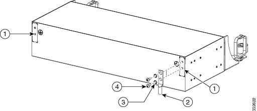
- Install the patch panel on the appropriate rack equipment:
- Establish grounding for the patch panel:
DETAILED STEPS
| Step 1 |
Mount the brackets on the patch panel (see the following figure):
|
||||||||
| Step 2 |
Install the patch panel on the appropriate rack equipment:
For information on mounting brackets and rack equipment, see Mounting Brackets and Rack Equipment. |
||||||||
| Step 3 |
Establish grounding for the patch panel:
For installing and routing fiber-optic and USB cables, see "Installing and Routing Fiber-Optic and USB Cables". For cleaning the fiber-optic connectors, see "Cleaning and Maintaining Fiber-Optic Connectors". |
Installing and Routing Fiber-Optic and USB Cables
The patch panel is passive and requires no power cabling or connections. All connectors are on the front panel and are equipped with LC/UPC bulkhead adapters and with a USB Type A receptacle connector for inventory purpose. For port label description, see "Table 1".
Warning |
Invisible laser radiation may be emitted from disconnected fibers or connectors. Do not stare into beams or view directly with optical instruments. Statement 1051 |
Caution |
When connecting an optical fiber patch cord between the patch panel and the optical card ports in a Cisco ONS 15454, use the electrostatic discharge wristband supplied with the ONS 15454. Plug the wristband into the ESD jack on the lower right front side of the ONS 15454. |
Note |
Always clean all fiber connectors thoroughly before making the connection with the mating adapter. Very small particles can permanently damage the end of the mating fiber inside the patch panel, which makes regular cleaning imperative. For cleaning instructions see "Cleaning and Maintaining Fiber-Optic Connectors". |
Caution |
The patch panel features LC/UPC bulkhead adapters for optical connections. Always use fiber-optic cables equipped with the corresponding (LC/UPC) connector type. Using any other type of connector results in damage to the connector or adapter, or both. |
SUMMARY STEPS
- To connect the fibers as appropriate (see the following figure):
- To secure the fibers, bundle the fibers using one of the four velcro strips that is provided (see the following figure):
- To connect and secure the inventory USB Type A plug connector to the inventory USB Type A receptacle connector (see the following figure):
DETAILED STEPS
| Step 1 |
To connect the fibers as appropriate (see the following figure):
|
||||||||||||
| Step 2 |
To secure the fibers, bundle the fibers using one of the four velcro strips that is provided (see the following figure): 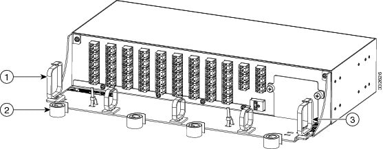
|
||||||||||||
| Step 3 |
To connect and secure the inventory USB Type A plug connector to the inventory USB Type A receptacle connector (see the following figure):
|
Uninstalling the Cisco ONS 15216 MD Odd and Even Patch Panels
SUMMARY STEPS
- Gently disconnect the fiber-optic connectors from the LC-LC adapters.
- Disconnect the inventory USB cable releasing it from the USB tie-wrap and from the USB receptacle.
- Remove the fibers and the USB cable from the fiber holder clips.
- Disconnect the ground lug.
- Loosen the mounting screws and remove the patch panel from the rack.
DETAILED STEPS
| Step 1 |
Gently disconnect the fiber-optic connectors from the LC-LC adapters. |
| Step 2 |
Disconnect the inventory USB cable releasing it from the USB tie-wrap and from the USB receptacle. |
| Step 3 |
Remove the fibers and the USB cable from the fiber holder clips. |
| Step 4 |
Disconnect the ground lug. |
| Step 5 |
Loosen the mounting screws and remove the patch panel from the rack. |
Cleaning and Maintaining Fiber-Optic Connectors
Connector cleaning is required to maintain the performance of fiber-optic circuits. It is important that both the LC/UPC connector at the end of the fiber-optic cable and the optical mating adapter on the front panel of the device are clean before the connection is made.
Warning |
Invisible laser radiation may be emitted from disconnected fibers or connectors. Do not stare into beams or view directly with optical instruments. Statement 1051 |
The following warning applies to disposal of chemicals and other materials used to clean connectors and adapters:
Warning |
Ultimate disposal of this product should be handled according to all national laws and regulations. Statement 1040 |
Note |
Before installing the fiber-optic cable, always perform the cleaning procedure for cable connectors described in the following section. Whenever possible, inspect each connector before connecting it to the optical mating adapter on the front panel. |
Note |
The LC optical mating adapter on the faceplate of the device is less likely to get dirty if it is capped when not in use. On some devices, the optical mating adapter has a shutter. The shutter automatically closes when the LC/UPC connector is disconnected. This prevents entry of dirt. The procedure for a thorough cleaning of these adapters is complicated. Use a commercially available cleaning kit and closely follow the instructions included with the kit. |
Customer-supplied Cleaning Materials
The Type A fiber optic connector cleaners (for example, CLETOP reel) are recommended to clean the cable connectors, but are not supplied with the device.
If properly maintained (only used with clean, defect-free fiber connectors and capped when not in use), the mating adapter would not require cleaning. However, if you suspect the adapter is dirty, clean it by using the CLETOP stick swab.
Note |
For multifiber cable assemblies, use specific cleaning tools or materials designed for the assembly type. |
Cleaning the Optical Mating Adapter
SUMMARY STEPS
- Read the cartridge cleaning instructions (provided by the manufacturer) to insert the cartridge cleaning tip into the optical mating adapter.
- Slide the lever on the cartridge to swipe the mating surface.
DETAILED STEPS
| Step 1 |
Read the cartridge cleaning instructions (provided by the manufacturer) to insert the cartridge cleaning tip into the optical mating adapter. |
||
| Step 2 |
Slide the lever on the cartridge to swipe the mating surface.
|
Cleaning Fiber-Optic Cable Connectors
-
Inspection microscope
-
Type A Fiber Optic Connector Cleaner (CLETOP reel)
-
Optical swab
-
Optical receiver cleaning stick
SUMMARY STEPS
- Using an inspection microscope, inspect each fiber connector for dirt, cracks, or scratches.
- Replace any damaged fiber connectors.
- Clean the fiber connectors with CLETOP reel:
DETAILED STEPS
| Step 1 |
Using an inspection microscope, inspect each fiber connector for dirt, cracks, or scratches. |
||||
| Step 2 |
Replace any damaged fiber connectors.
|
||||
| Step 3 |
Clean the fiber connectors with CLETOP reel:
|
Cisco ONS 15216 MD Patch Panel Specifications
This section contains environmental, power, optical, mechanical, and connector specifications for the patch panel.
Environmental and Power Specifications
| Environmental Condition | Minimum | Maximum | Units |
|---|---|---|---|
| Continuous Operative Temperature Range (OTR) | -5 | 65 | Celsius |
| 23 | 149 | Fahrenheit | |
| Power handling for the optical port | 300 | — | mW |
| Power handling for the USB Port | 400 | 600 | mW |
| Environmental Condition | Minimum | Maximum | Units |
|---|---|---|---|
| Storage Temperature Range | -40 | 85 | Celsius |
| -40 | 185 | Fahrenheit | |
| Continuous Operative Temperature Range (OTR) | -5 | 65 | Celsius |
| 23 | 149 | Fahrenheit | |
| Operating Humidity | 5 | 95 | %RH |
| Power handling for the each port | 500 | — | mW |
Optical Specifications
| Parameter | Condition | Min | Max | Units |
|---|---|---|---|---|
| Frequency/Wavelength Range (Odd Grid version) | Within operative temperature range | 196.1 | 191.4 | THz |
| 1566.31 | 1528.77 | nm | ||
| Frequency/Wavelength Range (Even Grid version | Within operative temperature range | 196.05 | 191.35 | THz |
| 1566.72 | 1529.16 | nm | ||
| Channel Spacing (Odd and Even Grid) | Within operative temperature range | 100 | GHz | |
| Operating Bandwidth | -20 | +20 | GHz | |
| -0.50 dB Clear Bandwidth |
|
-18 | +18 | GHz |
| -1.0 dB Clear Bandwidth | -23 | +23 | GHz | |
| -3.0 dB Clear Bandwidth | -32 | +32 | GHz | |
| Insertion Loss BOL1 (Beginning of life) - DEMUX module |
|
3.0 | 6.0 | dB |
| Insertion Loss BOL (Beginning of life) - MUX module | 4.0 | 6.0 | dB | |
| Insertion Loss EOL (End of life) - DEMUX module | 3.0 | 6.5 | dB | |
| 4.0 | 6.5 | dB | ||
| Insertion Loss EOL (End of life) - MUX module | ||||
| Insertion Loss Uniformity2 | — | 1.5 | dB | |
| Adjacent Channel Isolation3 DEMUX |
|
20.0 | — | dB |
| Non-Adjacent Channel Isolation4 DEMUX | 30.0 | — | dB | |
| Total Crosstalk DEMUX | 16.0 | — | dB | |
| Adjacent Channel Isolation MUX |
|
17.0 | — | dB |
| Non-Adjacent Channel Isolation MUX | 30.0 | — | dB | |
| Total Crosstalk MUX | 14.0 | — | dB | |
| Group Delay Ripple5 (GDR) |
|
-1.0 | +1.0 | ps |
| Chromatic Dispersion6 | -12.0 | +12.0 | ps/nm | |
| Return Loss | 40 | — | ||
| Polarization Dependent Loss (PDL)7 | — | 0.7 | dB | |
| Polarization Mode Dispersion (PMD)8 | — | 0.5 | ps | |
| Monitor Attenuation MUX9 | 18 | 22 | dB | |
| Monitor Attenuation DEMUX10 | 18 | 22 | dB | |
| AUX-MUX to COM-TX Insertion Loss | — | 11 | dB | |
| Parameter | Condition | Min | Max | Units |
|---|---|---|---|---|
| Frequency/Wavelength Range (Odd Grid version) | Within operative temperature range | 196.1 | 191.4 | THz |
| 1566.31 | 1528.77 | nm | ||
| Frequency/Wavelength Range (Even Grid version | Within operative temperature range | 196.05 | 191.35 | THz |
| 1566.72 | 1529.16 | nm | ||
| Channel Spacing (Odd and Even Grid) | Within operative temperature range | 100 | GHz | |
| Operating Bandwidth | -33 | +33 | GHz | |
| -1.5 dB Clear Bandwidth |
|
-30 | 30 | GHz |
| -3.0 dB Clear Bandwidth | -37.5 | +37.5 | GHz | |
| Insertion Loss BOL11 (Beginning of life) - DEMUX module |
|
3.0 | 5.0 | dB |
| Insertion Loss BOL (Beginning of life) - MUX module | 3.0 | 5.0 | dB | |
| Insertion Loss EOL (End of life) - DEMUX module | 3.0 | 5.5 | dB | |
| 3.0 | 5.5 | dB | ||
| Insertion Loss EOL (End of life) - MUX module | ||||
| Insertion Loss Uniformity12 | — | 1 | dB | |
| Adjacent Channel Isolation13 DEMUX |
|
8.0 | — | dB |
| Non-Adjacent Channel Isolation14 DEMUX | 25.0 | — | dB | |
| Total Crosstalk DEMUX | 5.0 | — | dB | |
| Adjacent Channel Isolation MUX |
|
8.0 | — | dB |
| Non-Adjacent Channel Isolation MUX | 25.0 | — | dB | |
| Total Crosstalk MUX | 5.0 | — | dB | |
| Group Delay Ripple15 (GDR) |
|
0 | 3 | ps |
| Chromatic Dispersion16 | -12.0 | +12.0 | ps/nm | |
| Return Loss | 40 | — | ||
| Polarization Dependent Loss (PDL)17 | — | 0.7 | dB | |
| Polarization Mode Dispersion (PMD)18 | — | 0.5 | ps | |
| Monitor Attenuation MUX19 | 18 | 22 | dB | |
| Monitor Attenuation DEMUX20 | 18 | 22 | dB | |
| AUX-RX to COM-TX Insertion Loss MUX | — | 11 | dB | |
Connector and Mechanical Specifications
| Parameter | Condition | Specification |
|---|---|---|
| Connector Type | All optical ports | LC/UPC II |
| USB inventory port | USB Type A receptacle connector | |
| Optical Adapter Type | All optical ports | LC |
| Patch Panel Dimensions | The Cisco ONS 15216 MD odd or even patch panels measure 3.45-inches (87.6 mm) high, 17.21-inches (437.1 mm) wide, and 10.96-inches (278.4 mm) deep | |
Related Documentation
Use this guide in conjunction with the following referenced publications:
-
Cisco ONS 15454 DWDM Configuration Guides
-
Cisco ONS 15454 DWDM Troubleshooting Guide
Short Description
Cisco and the Cisco logo are trademarks or registered trademarks of Cisco and/or its affiliates in the U.S. and other countries. To view a list of Cisco trademarks, go to this URL: https://www.cisco.com/c/en/us/about/legal/trademarks.html. Third-party trademarks mentioned are the property of their respective owners. The use of the word partner does not imply a partnership relationship between Cisco and any other company. (1721R)
Obtaining Documentation and Submitting a Service Request
For information on obtaining documentation, submitting a service request, and gathering additional information, see the monthly What's New in Cisco Product Documentation, which also lists all new and revised Cisco technical documentation, at: http://www.cisco.com/en/US/docs/general/whatsnew/whatsnew.html
Subscribe to the What's New in Cisco Product Documentation as a Really Simple Syndication (RSS) feed and set content to be delivered directly to your desktop using a reader application. The RSS feeds are a free service and Cisco currently supports RSS version 2.0.
Cisco and the Cisco logo are trademarks or registered trademarks of Cisco and/or its affiliates in the U.S. and other countries. To view a list of Cisco trademarks, go to this URL: https://www.cisco.com/c/en/us/about/legal/trademarks.html. Third-party trademarks mentioned are the property of their respective owners. The use of the word partner does not imply a partnership relationship between Cisco and any other company. (1721R)
 Feedback