Memory Replacement Instructions for the Network Processing Engine or Network Services Engine and Input/Output Controller
Bias-Free Language
The documentation set for this product strives to use bias-free language. For the purposes of this documentation set, bias-free is defined as language that does not imply discrimination based on age, disability, gender, racial identity, ethnic identity, sexual orientation, socioeconomic status, and intersectionality. Exceptions may be present in the documentation due to language that is hardcoded in the user interfaces of the product software, language used based on RFP documentation, or language that is used by a referenced third-party product. Learn more about how Cisco is using Inclusive Language.
- Updated:
- September 22, 2006
Chapter: SDRAM and DRAM Memory Systems Overview
SDRAM and DRAM Memory Systems Overview
Product Numbers: MEM-NPE-32MB=, MEM-NPE-64MB=, MEM-NPE-128MB=, MEM-SD-NPE-32MB=, MEM-SD-NPE-64MB=, MEM-SD-NPE-128MB=, MEM-SD-NSE-256MB=, MEM-NPE-400-128MB=, MEM-NPE-400-256MB=, MEM-NPE-400-512MB=, NPE-100=, NPE-150=, NPE-175=, NPE-200=, NPE-225=, NPE-300=, NPE-400=, NSE-1=, NPE-G1=, UBR7200-NPE-G1=, NPE-G2=, UBR7200-NPE-G2
The Cisco 7200 series and Cisco uBR7200 series memory systems are part of the network processing engine or network services engine. The network processing engine is available in nine versions: the NPE-100, NPE-150, NPE-175, NPE-200, NPE-225, NPE-300, NPE-400, NPE-G1 and NPE-G2. The network services engine is available in one version, the NSE-1.
http://www.cisco.com/en/US/products/hw/routers/ps341/prod_bulletins_list.html.

Note ![]() The Cisco uBR7246VXR universal broadband router does not support the NPE-G1 or NPE-G2 processor but must use the UBR7200-NPE-G1or UBR7200-NPE-G2 processor, which contains the bootflash code required to boot the router. Unless otherwise indicated, all references to NPE-G1 or NPE-G2 in this document also refer to the UBR7200-NPE-G1 or UBR7200-NPE-G2 rocessor.
The Cisco uBR7246VXR universal broadband router does not support the NPE-G1 or NPE-G2 processor but must use the UBR7200-NPE-G1or UBR7200-NPE-G2 processor, which contains the bootflash code required to boot the router. Unless otherwise indicated, all references to NPE-G1 or NPE-G2 in this document also refer to the UBR7200-NPE-G1 or UBR7200-NPE-G2 rocessor.
Table 2-1 shows the current network processing engine or network services engine options and restrictions for Cisco 7200 series and Cisco uBR7200 series routers. Table 2-2 shows the network processing engine options for Cisco 7200 series and Cisco uBR7200 series routers that have reached their end-of-life and are no longer sold, but are still supported in existing installations.
|
|
|
|
|
|
|
|---|---|---|---|---|---|
Cisco 7200 series |
|||||
• |
Yes |
Yes |
Yes |
Yes |
Yes |
• |
No |
No |
No |
No |
Yes |
Cisco AS5800 |
|||||
• |
No |
No |
No |
Yes |
— |
• |
No |
No |
No |
No |
— |
Cisco uBR7200 series |
|||||
• |
Yes1 |
Yes2 |
No |
Yes |
Yes |
• |
No |
No |
No |
No |
Yes |
1 The Cisco uBR7246VXR router cannot use the NPE-G2 processor but must use the UBR7200-NPE-G2 processor. 2 The Cisco uBR7246VXR router cannot use the NPE-G1 processor but must use the UBR7200-NPE-G1 processor. |
|
|
|
|
|
|
|
|---|---|---|---|---|---|
Cisco 7200 series |
|||||
• |
Yes |
Yes |
Yes |
Yes |
Yes |
• |
No |
Yes |
Yes |
Yes |
Yes |
Cisco AS5800 |
|||||
• |
Yes |
Yes |
— |
— |
— |
• |
No |
Yes |
— |
— |
— |
Cisco uBR7200 series |
|||||
• |
Yes |
No |
No |
No |
— |
• |
No |
Yes |
No |
Yes |
— |
1 Previous documents stated that the NPE-175 was also supported on the Cisco uBR7200 series routers. Because the NPE-175 has reached its end of life and was never made orderable on the Cisco uBR7200 series routers, it is no longer shown as supported on the Cisco uBR7200 series routers. |
The memory systems provide the following functions:
•![]() Main memory (DRAM in the NPE-100, NPE-150, and NPE-200; SDRAM in the NPE-175, NPE-225, NPE-300, NPE-400, NSE-1, NPE-G1, and NPE-G2)—Stores the running configuration and routing tables. The Cisco IOS software executes from main memory.
Main memory (DRAM in the NPE-100, NPE-150, and NPE-200; SDRAM in the NPE-175, NPE-225, NPE-300, NPE-400, NSE-1, NPE-G1, and NPE-G2)—Stores the running configuration and routing tables. The Cisco IOS software executes from main memory.
•![]() Shared memory—Used for packet buffering by the router's network interfaces.
Shared memory—Used for packet buffering by the router's network interfaces.
•![]() Flash memory—Stores the boot helper image software. The boot helper image allows you to boot the router when PC cards do not contain a valid system image. It also allows you to boot the router from a network server.
Flash memory—Stores the boot helper image software. The boot helper image allows you to boot the router when PC cards do not contain a valid system image. It also allows you to boot the router from a network server.
•![]() CompactFlash Disks, Flash Disks, or PC cards—Stores the default Cisco IOS software image.
CompactFlash Disks, Flash Disks, or PC cards—Stores the default Cisco IOS software image.
•![]() Boot erasable programmable read-only memory (EPROM)—Does power-on diagnostics and initialization; initiates system boot-up based on virtual configuration register. Contains the ROM monitor, which permits you to boot the Cisco IOS image from a CompactFlash Disk, Flask Disk, or PC card if a boot helper image is not present in the Flash memory.
Boot erasable programmable read-only memory (EPROM)—Does power-on diagnostics and initialization; initiates system boot-up based on virtual configuration register. Contains the ROM monitor, which permits you to boot the Cisco IOS image from a CompactFlash Disk, Flask Disk, or PC card if a boot helper image is not present in the Flash memory.
•![]() Nonvolatile random-access memory (NVRAM)—Stores the system configuration, environmental monitoring logs, and the virtual configuration register.
Nonvolatile random-access memory (NVRAM)—Stores the system configuration, environmental monitoring logs, and the virtual configuration register.
Terms and Acronyms
•![]() Cache memory—Memory with fast access and small capacity used to temporarily store recently accessed data; found either incorporated into the processor or near it.
Cache memory—Memory with fast access and small capacity used to temporarily store recently accessed data; found either incorporated into the processor or near it.
•![]() DIMM—dual in-line memory module
DIMM—dual in-line memory module
•![]() DRAM—dynamic random-access memory
DRAM—dynamic random-access memory
•![]() Instruction and data cache memory—Instructions to the processor, and data on which the instructions work.
Instruction and data cache memory—Instructions to the processor, and data on which the instructions work.
•![]() Integrated cache—Cache that is built into the processor; sometimes referred to as internal cache. Cache memory physically located outside the processor is not integrated, and is sometimes referred to as external cache.
Integrated cache—Cache that is built into the processor; sometimes referred to as internal cache. Cache memory physically located outside the processor is not integrated, and is sometimes referred to as external cache.
•![]() Primary, secondary, tertiary cache memory—Hierarchical cache memory storage based on the proximity of the cache to the core of the processor. Primary cache is closest to the processor core and has the fastest access. Secondary cache has slower access than primary cache, but faster access than tertiary cache.
Primary, secondary, tertiary cache memory—Hierarchical cache memory storage based on the proximity of the cache to the core of the processor. Primary cache is closest to the processor core and has the fastest access. Secondary cache has slower access than primary cache, but faster access than tertiary cache.
•![]() OTP—one time programmable
OTP—one time programmable
•![]() RAM—random-access memory
RAM—random-access memory
•![]() RISC—reduced instruction set computing
RISC—reduced instruction set computing
•![]() ROM—read-only memory
ROM—read-only memory
•![]() SIMM—single in-line memory module
SIMM—single in-line memory module
•![]() SODIMM—small outline dual in-line memory module
SODIMM—small outline dual in-line memory module
•![]() SDRAM—synchronous dynamic random-access memory
SDRAM—synchronous dynamic random-access memory
•![]() SDRAM-fixed—SDRAM that is a fixed size or quantity; can be replaced, but not upgraded.
SDRAM-fixed—SDRAM that is a fixed size or quantity; can be replaced, but not upgraded.
•![]() SRAM—static random-access memory
SRAM—static random-access memory
•![]() Unified cache—Instruction cache and data cache are combined. For example, a processor may have primary cache with separate instruction and data cache memory, but unified secondary cache.
Unified cache—Instruction cache and data cache are combined. For example, a processor may have primary cache with separate instruction and data cache memory, but unified secondary cache.
Network Processing Engine or Network Services Engine Memory Information
Refer to figures and tables for memory location specifications, and configurations for the network processing engine or the network services engine on these pages:
•![]() NPE-G2 and UBR7200-NPE-G2 Memory Information
NPE-G2 and UBR7200-NPE-G2 Memory Information
•![]() NPE-G1 and UBR7200-NPE-G1 Memory Information
NPE-G1 and UBR7200-NPE-G1 Memory Information
•![]() NPE-225 and NPE-175 Memory Information
NPE-225 and NPE-175 Memory Information
For removal and installation information, follow the instructions in Chapter 3, "Preparing for Installation" and Chapter 4, "Installing and Removing SDRAM and DRAM."
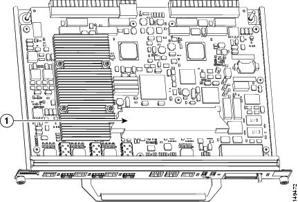
NPE-G2 and UBR7200-NPE-G2 Memory Information
Use the following figure and tables for information about the NPE-G2 memory location, specifications, and configurations.
Figure 2-1 NPE-G2 and UBR7200-NPE-G2
|
|
DIMM |
|
|
|
|
|
|---|---|---|---|
1 GB |
S1 |
1-GB DIMM |
MEM-NPE-G2-1GB= |
2 GB |
S1 |
2-GB DIMM |
MEM-NPE-G2-2GB= |
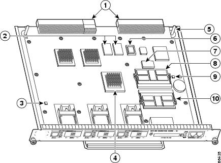
NPE-G1 and UBR7200-NPE-G1 Memory Information
Use the following figure and tables for information about the NPE-G1 and UBR7200-NPE-G1 memory location, specifications, and configurations.
Figure 2-2 NPE-G1 and UBR7200-NPE-G1
|
|
Midplane connectors |
|
Boot ROM (U1) |
|
|
Flash memory |
|
NVRAM (U7) |
|
|
Temperature sensor |
|
SODIMM 2 (J4) |
|
|
BCM 1250 processor (U22) |
|
Temperature sensor |
|
|
Keying post |
|
SODIMM 1 (J3) |
|
|
|
|
|
|
|---|---|---|---|---|
SDRAM |
128MB, 256MB, |
2 |
128-MB, 256-MB, or 512-MB SODIMMs—Requires two SODIMMs of the same size to create the total memory size of 256 MB, 512 MB, or 1024 MB (see Table 2-6) |
J3 and J4 |
Boot ROM |
512 KB |
1 |
Reprogrammable Boot ROM for the ROM monitor program |
U1 |
Flash memory |
16 MB |
1 |
Contains the default boot helper (boot loader) image1 |
U25 and U26 |
NVRAM |
512 KB |
1 |
Nonvolatile EPROM for the system configuration file |
U7 |
Primary cache |
32 KB (16 KB instruction, 16 KB data) |
— |
BCM 1250 processor internal cache |
U22 |
Secondary cache |
512 KB |
— |
BCM 1250 system unified, internal cache |
U22 |
1 The NPE-G1 and UBR7200-NPE-G1 processors contain different boothelper images to support the Cisco 7200 series and Cisco uBR7200 series routers, respectively. |
|
|
|
|
|
|---|---|---|---|
256 MB (default) |
J3 and J4 |
2 128-MB SODIMMs |
MEM-NPE-G1-256MB |
512 MB |
J3 and J4 |
2 256-MB SODIMMs |
MEM-NPE-G1-512MB |
1 GB |
J3 and J4 |
2 512-MB SODIMMs |
MEM-NPE-G1-1GB |
1 The same-sized SODIMM must be installed in each bank. |
NSE-1 Memory Information
Use the following figure and tables for information about the NSE-1 memory location, specifications, and configurations.
Figure 2-3 NSE-1
|
|
|
|
|
|
|
|---|---|---|---|---|---|
RM7000 processor |
— |
— |
1 |
262-MHz RM7000 RISC |
U22 |
PXF processor |
— |
— |
1 |
— |
U34 |
SDRAM |
128, 256 MB |
1 |
128- or 256-MB DIMM |
U15 |
|
Boot ROM |
512 KB |
1 |
OTP1 ROM for the ROM monitor program |
U1 |
|
Primary cache |
16 KB (instruction), 16 KB (data) |
— |
RM7000 processor internal cache |
U22 |
|
Secondary cache |
256 KB |
— |
RM7000 processor internal, unified instruction and data cache |
U22 |
|
Tertiary cache |
2 MB (fixed) |
— |
RM7000 processor external cache |
U7, U9, U12, U14, U17 |
1 OTP = one time programmable |
|
|
|
|
|
|---|---|---|---|
128 MB |
U15 |
1 128-MB DIMM |
MEM-SD-NPE-128MB |
256 MB |
U15 |
1 256-MB DIMM |
MEM-SD-NSE-256MB |
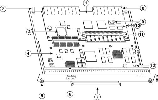
NPE-400 Memory Information
Use the following figure and tables for information about the NPE-400 memory location, specifications, and configurations.
Note ![]() The NPE-400 uses a single small outline dual in-line memory module (SODIMM).
The NPE-400 uses a single small outline dual in-line memory module (SODIMM).
Figure 2-4 NPE-400
NPE-300 Memory Information
Use the following figure and tables for information about the NPE-300 memory location, specifications, and configurations.
Note ![]() The NPE-300 contains two banks of SDRAM. Both SDRAM banks are used for all packet memory requirements; however, bank 0 is used exclusively for packet memory and is set at a fixed configuration in the factory.
The NPE-300 contains two banks of SDRAM. Both SDRAM banks are used for all packet memory requirements; however, bank 0 is used exclusively for packet memory and is set at a fixed configuration in the factory.
Bank 1 contains two user-configurable SDRAM slots, DIMM slot 2 and DIMM slot 3. (See Figure 2-5.) Both slots in bank 1 can be populated by DIMMs of different sizes; however, the size of the DIMM in slot 2 must be greater than or equal to the size of the DIMM in slot 3, and the size of the DIMM in slot 3 can be zero.
Figure 2-5 NPE-300
|
|
|
|
|
|
|
|---|---|---|---|---|---|
RM7000 |
— |
— |
1 |
262-MHz RM7000 RISC |
U49 |
Fixed SDRAM |
32-MB |
1 |
32- MB DIMM |
Bank 01 : U16 |
|
Configurable SDRAM |
32 to 256 MB |
1 configurable bank with 2 SDRAM slots |
32-, 64-, 128-, or 256-MB DIMMs (based on maximum SDRAM required) |
Bank 1: U45 and U44 |
|
Boot ROM |
512 KB |
1 |
OTP2 ROM for the ROM monitor program |
Socket U13 |
|
Primary cache |
16 KB (instruction), 16 KB (data) |
— |
RM7000 processor internal cache |
U49 |
|
Secondary cache |
256 KB |
— |
RM7000 processor unified, internal cache |
U49 |
|
Tertiary cache |
2 MB (fixed) |
— |
RM7000 processor external cache |
U7, U8, U9, U10, U17 |
1 Socket U15 is never populated, although it is part of bank 0. 2 OTP = one time programmable 3 Located on the processor engine board |
|
|
|
|
|
|---|---|---|---|
32 MB4 + 32 MB |
U45 (DIMM slot 2 only) |
1 32-MB DIMM |
MEM-SD-NPE-32MB |
32 MB4 + 64 MB |
U45 and U44 |
2 32-MB DIMMs |
MEM-SD-NPE-32MB |
U45 |
1 64-MB DIMM |
MEM-SD-NPE-64MB |
|
32 MB4 + 128 MB |
U45 and U44 |
2 64-MB DIMMs |
MEM-SD-NPE-64MB |
U45 |
1 128-MB DIMM |
MEM-SD-NPE-128MB |
|
32 MB4 + 256 MB |
U45 and U44 |
2 128-MB DIMMs |
MEM-SD-NPE-256MB |
U45 |
1 256-MB DIMM |
MEM-SD-NSE-256MB |
1 Refer to the Cisco AS5800 Universal Access Server documentation on Cisco.com for Cisco AS5800 Universal Access Server SDRAM options. 2 There are two user-upgradable SDRAM slots in bank 1. (Bank 0 is used exclusively for packet memory and is set at a fixed configuration in the factory.) 3 These products are also available as SDRAM upgrades. To order an upgrade, add an equal sign (=) after the Product Number, for example, MEM-SD-NPE-128MB=. 4 This 32 MB is fixed memory in SDRAM bank 0. |
NPE-225 and NPE-175 Memory Information
Use the following figure and tables for information about the NPE-225 and NPE-175 memory location, specifications, and configurations.
Figure 2-6 NPE-225
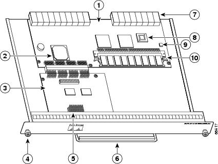
Figure 2-7 NPE-175

|
|
|
|
|
|
|
|---|---|---|---|---|---|
NPE-175 - R5270 |
— |
— |
1 |
R5270 200-MHz RISC1 |
U4 |
NPE-225 - R5271 |
— |
— |
1 |
R5271 262-MHz RISC |
U4 |
SDRAM |
64, 128, or 256 MB2 |
1 configurable bank with 1 SDRAM slot |
DIMM |
U15 |
|
Boot ROM |
512 KB |
1 |
OTP3 ROM for the ROM monitor program |
U1 |
|
Primary cache |
16 KB (instruction), |
— |
R5270 processor internal cache |
U4 |
|
32 KB (instruction), |
— |
R5271 processor internal cache |
U4 |
||
Secondary cache |
2 MB |
4 chips, each 512 KB by 8 bits wide |
R527x processor unified, external cache |
U5, U6, U7, U84 |
1 RISC = reduced instruction set computing 2 256 MB supported on the NPE-225 processor only 3 OTP = one time programmable 4 Located on the processor engine board |
|
|
|
|
|
|---|---|---|---|
64 MB1 |
U15 |
1 64-MB DIMM |
MEM-SD-NPE-64MB |
128 MB |
U15 |
1 128-MB DIMM |
MEM-SD-NPE-128MB |
256 MB |
U15 |
1 256-MB DIMM |
MEM-SD-NSE-256MB |
1 The 64-MB memory configuration is not supported on the NPE-225 on a Cisco uBR7200 series router, which requires a minimum of 128 MB memory. The 64-MB memory configuration is supported on the Cisco 7200 series routers, but 128 MB is the minimum recommended memory configuration. |
|
|
|
|
|
|---|---|---|---|
64 MB |
U15 |
1 64-MB DIMM |
MEM-SD-NPE-64MB |
128 MB |
U15 |
1 128-MB DIMM |
MEM-SD-NPE-128MB |
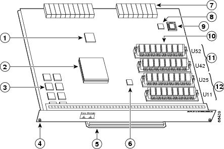
NPE-200 Memory Information
Note ![]() To prevent DRAM errors in the NPE-200and to ensure that your system initializes correctly at startup, DRAM bank 0 (socket U18 and U25, or U11 and U25) must contain no fewer than two SIMMs of the same type. You can also install two SIMMs of the same type in bank 1 (socket U4 and U12, or U42 and U52); however, bank 0 must always contain the two largest SIMMs.
To prevent DRAM errors in the NPE-200and to ensure that your system initializes correctly at startup, DRAM bank 0 (socket U18 and U25, or U11 and U25) must contain no fewer than two SIMMs of the same type. You can also install two SIMMs of the same type in bank 1 (socket U4 and U12, or U42 and U52); however, bank 0 must always contain the two largest SIMMs.
Use the following figure and tables for information about the NPE-200 memory location, specifications, and configurations.
Figure 2-8 NPE-200
|
|
|
|
|
|
|
|---|---|---|---|---|---|
R5000 |
1 |
R5000 200-MHz RISC1 |
U44 |
||
DRAM2 |
32 to 128 MB |
2 to 4 |
16- or 32-MB SIMMs (based on maximum DRAM required) |
Bank 0: U11 and U25 |
|
SRAM3 |
4 MB |
8 |
8 chips, each being 512 KB x 8 bits wide |
U6, U10, U13, U14, U28, U29, U38, and U39 |
|
Boot ROM4 |
256 KB |
1 |
EPROM5 for the ROM monitor program |
U92 |
|
Primary cache |
— |
— |
R5000 internal cache |
U44 |
1 RISC = reduced instruction set computing 2 DRAM = dynamic random-access memory 3 SRAM = static random-access memory 4 ROM = read-only memory 5 EPROM = erasable programmable read-only memory |
|
|
|
|
|
|
|
|---|---|---|---|---|---|
32 MB |
U11 and U25 |
2 16-MB SIMMs |
U42 and U52 |
— |
MEM-NPE-32MB2 |
64 MB |
U11 and U25 |
2 32-MB SIMMs |
U42 and U52 |
— |
MEM-NPE-64MB2 |
128 MB |
U11 and U25 |
2 32-MB SIMMs |
U42 and U52 |
2 32-MB SIMMs |
MEM-NPE-128MB2 |
1 Refer to the Cisco AS5800 Universal Access Server documentation listed on Ciso.com for Cisco AS5800 Universal Access Server DRAM options. 2 These products are also available as DRAM upgrades. For example, to upgrade a network processing engine from 32 MB to 64 MB of DRAM, order Product Number MEM-NPE-64MB=. |
NPE-150 Memory Information
Note ![]() To prevent DRAM errors in the NPE-150 and to ensure that your system initializes correctly at startup, DRAM bank 0 (socket U18 and U25, or U11 and U25) must contain no fewer than two SIMMs of the same type. You can also install two SIMMs of the same type in bank 1 (socket U4 and U12, or U42 and U52); however, bank 0 must always contain the two largest SIMMs.
To prevent DRAM errors in the NPE-150 and to ensure that your system initializes correctly at startup, DRAM bank 0 (socket U18 and U25, or U11 and U25) must contain no fewer than two SIMMs of the same type. You can also install two SIMMs of the same type in bank 1 (socket U4 and U12, or U42 and U52); however, bank 0 must always contain the two largest SIMMs.
Use the following figure and tables for information about the NPE-150 memory location, specifications, and configurations.
Figure 2-9 NPE-150
|
|
|
|
|
|
|
|---|---|---|---|---|---|
R4700 |
1 |
R4700 150-MHz RISC1 |
U201 |
||
DRAM2 (Main memory) |
32 to 128 MB |
2 to 4 |
16- or 32-MB SIMMs (based on maximum DRAM required) |
Bank 0: U18 and U25 |
|
SRAM3 |
1 MB |
8 |
8 chips, each being 128 KB x 9 bits wide |
U700 through U703 |
|
Primary cache |
— |
— |
R4700 internal cache |
U201 |
|
Secondary cache |
512 KB |
4 |
R4700 unified, external cache |
U2, U10, U14, and U26 |
1 RISC = reduced instruction set computing 2 DRAM = dynamic random-access memory 3 SRAM = static random-access memory |
|
|
|
|
|
|
|
|---|---|---|---|---|---|
32 MB |
U18 and U25 |
2 16-MB SIMMs |
U4 and U12 |
— |
MEM-NPE-32MB |
64 MB |
U18 and U25 |
2 32-MB SIMMs |
U4 and U12 |
— |
MEM-NPE-64MB2 |
128 MB |
U18 and U25 |
2 32-MB SIMMs |
U4 and U12 |
2 32-MB SIMMs |
MEM-NPE-128MB |
1 Refer to the Cisco AS5800 Universal Access Server documentation listed on Cisco.co m for Cisco AS5800 Universal Access Server DRAM options. 2 These products are also available as DRAM upgrades. For example, to upgrade a network processing engine from 32 MB to 64 MB of DRAM, order Product Number MEM-NPE-64MB=. |
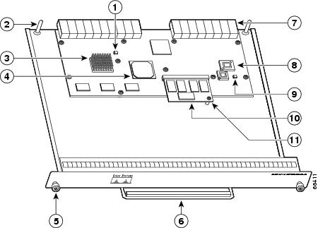
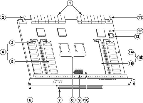
NPE-100 Memory Information
Note ![]() To prevent DRAM errors in the NPE-100, and to ensure that your system initializes correctly at startup, DRAM bank 0 (socket U18 and U25, or U11 and U25) must contain no fewer than two SIMMs of the same type. You can also install two SIMMs of the same type in bank 1 (socket U4 and U12, or U42 and U52); however, bank 0 must always contain the two largest SIMMs.
To prevent DRAM errors in the NPE-100, and to ensure that your system initializes correctly at startup, DRAM bank 0 (socket U18 and U25, or U11 and U25) must contain no fewer than two SIMMs of the same type. You can also install two SIMMs of the same type in bank 1 (socket U4 and U12, or U42 and U52); however, bank 0 must always contain the two largest SIMMs.
Use the following figure and tables for information about the NPE-100 memory location, specifications, and configurations.
Figure 2-10 NPE-100
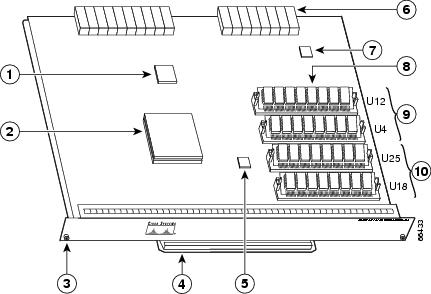
|
|
System controller |
|
Midplane connectors |
|
|
R4700 microprocessor |
|
Temperature sensor |
|
|
Captive installation screw |
|
DRAM SIMMs |
|
|
Handle |
|
Bank 1 |
|
|
Temperature sensor |
|
Bank 0 |
|
|
|
|
|
|
|
|---|---|---|---|---|---|
R4700 |
1 |
R4700 150-MHz RISC1 |
U201 |
||
DRAM2 |
32 to 128 MB |
2 to 4 |
16- or 32-MB SIMMs (based on maximum DRAM required) |
Bank 0: U18 and U25 Bank 1: U4 and U12 |
|
Primary cache |
— |
— |
R4700 internal cache |
U201 |
|
Secondary cache |
512 KB |
4 |
R4700 unified, external cache |
U2, U10, U14, and U26 |
1 RISC = reduced instruction set computing 2 DRAM = dynamic random-access memory |
|
|
|
|
|
|
Product Number2 |
|---|---|---|---|---|---|
32 MB |
U18 and U25 |
2 16-MB SIMMs |
U4 and U12 |
— |
MEM-NPE-32MB |
64 MB |
U18 and U25 |
2 32-MB SIMMs |
U4 and U12 |
— |
MEM-NPE-64MB |
128 MB |
U18 and U25 |
2 32-MB SIMMs |
U4 and U12 |
2 32-MB SIMMs |
MEM-NPE-128MB2 |
1 Refer to the Cisco AS5800 Universal Access Server documentation listed on Cisco.con for Cisco AS5800 Universal Access Server DRAM options. 2 These products are also available as DRAM upgrades. For example, to upgrade a network processing engine from 32 MB to 64 MB of DRAM, order Product Number MEM-NPE-64MB=. |
 Feedback