- Preface
- Cisco ONS Documentation Roadmap for Release 9.8.x
- New and Changed Information
- Chapter 1, Install the Cisco ONS 15454, ONS 15454 M2, and ONS 15454 M6 Shelf
- Chapter 2, Connecting the PC and Logging into the GUI
- Chapter 3, Install the Control Cards
- Chapter 4, Setup Optical Service Channel Cards
- Chapter 5, Optical Amplifier Cards
- Chapter 6, Provision Multiplexer and Demultiplexer Cards
- Chapter 7, Setup Tunable Dispersion Compensating Units
- Chapter 8, Provision Protection Switching Module
- Chapter 9, Optical Add/Drop Cards
- Chapter 10, Reconfigurable Optical Add/Drop Cards
- Chapter 11, Provision Transponder and Muxponder Cards
- Chapter 12, Node Reference
- Chapter 13, Network Reference
- Chapter 14, Turn Up a Node
- Chapter 15, Perform Node Acceptance Tests
- Chapter 16, Turn Up a Network
- Chapter 17, Create Optical Channel Circuits and Provisionable Patchcords
- Chapter 18, Monitor Performance
- Chapter 19, Manage the Node
- Chapter 20, Alarm and TCA Monitoring and Management
- Chapter 21, Change DWDM Card Settings
- Chapter 22, Manage Network Connectivity
- Chapter 23, Upgrade, Add, and Remove Cards and Nodes
- Chapter 24, Maintain the Node
- Chapter 25, Security Reference
- Chapter 26, Timing Reference
- Chapter 27, SNMP
- Appendix A, CTC Operation, Information, and Shortcuts
- Appendix B, Hardware Specifications
- Appendix C, Administrative and Service States
- Appendix D, Configure GE_XP, 10GE_XP, GE_XPE, and 10GE_XPE Cards Using PCLI
- Appendix E, Pseudo Command Line Interface Reference
- Appendix F, Fiber and Connector Losses in Raman Link Configuration
- Appendix G, Card Features
- Appendix H, Network Element Defaults
Cisco ONS 15454 DWDM Configuration Guide, Release 9.8.x
Bias-Free Language
The documentation set for this product strives to use bias-free language. For the purposes of this documentation set, bias-free is defined as language that does not imply discrimination based on age, disability, gender, racial identity, ethnic identity, sexual orientation, socioeconomic status, and intersectionality. Exceptions may be present in the documentation due to language that is hardcoded in the user interfaces of the product software, language used based on RFP documentation, or language that is used by a referenced third-party product. Learn more about how Cisco is using Inclusive Language.
- Updated:
- July 9, 2014
Chapter: Chapter 12, Node Reference
- 12.1 DWDM Node Configurations
- 12.2 Supported Node Configurations for OPT-RAMP-C and OPT-RAMP-CE Cards
- 12.3 Supported Node Configurations for PSM Card
- 12.4 Multishelf Node
- 12.5 Connecting Passive Modules to a ONS 15454 M2 or ONS 15454 M6 Node
- 12.6 Optical Sides
- 12.7 Configuring Mesh DWDM Networks
- 12.7.1 Line Termination Mesh Node Using 40-WXC-C Cards
- 12.7.1.1 40-Channel Omni-directional n-degree ROADM Node
- 12.7.1.2 40-Channel Colorless n-Degree ROADM Node
- 12.7.1.3 40-Channel Colorless and Omni-directional n-Degree ROADM Node
- 12.7.2 Line Termination Mesh Node Using 80-WXC-C Cards
- 12.7.2.1 80-Channel Omni-directional n-degree ROADM Node
- 12.7.2.2 80-Channel Colorless n-degree ROADM Node
- 12.7.2.3 80-Channel Colorless and Omni-directional n-Degree ROADM Node
- 12.7.3 Line Termination Mesh Node Using 40-SMR2-C Cards
- 12.7.4 XC Terminatio n Mesh Node
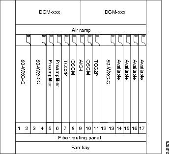
- 12.7.5 Mesh Patch Panels and Shelf Layouts
- 12.7.6 Using a Mesh Node With Omni-Directional Add/Drop Section
- 12.8 DWDM Node Cabling
- 12.8.1 OSC Link Termination Fiber-Optic Cabling
- 12.8.2 Hub Node Fiber-Optic Cabling
- 12.8.3 Terminal Node Fiber-Optic Cabling
- 12.8.4 Line Amplifier Node Fiber-Optic Cabling
- 12.8.5 OSC Regeneration Node Fiber-Optic Cabling
- 12.8.6 Amplified or Passive OADM Node Fiber-Optic Cabling
- 12.8.7 ROADM Node Fiber-Optic Cabling
- 12.9 Automatic Node Setup
- 12.10 DWDM Network Functional View
- 12.10.1 GMPLS Control Plane
- 12.10.1.1 Card Support
- 12.10.1.2 Acceptance Thresholds
- 12.10.1.3 Validation Modes
- 12.10.1.4 GMPLS Optical Restoration
- 12.10.1.5 Restoration Modes
- 12.10.1.6 Soak Time
- 12.10.1.7 Restoration Status
- 12.10.1.8 WSON Alarms
- 12.10.1.9 GMPLS UNI
- 12.10.2 DWDM Network Functional View (NFV)
- 12.10.2.1 Graphical View Pane
- 12.10.2.2 Overview Pane
- 12.10.2.3 Network Data Pane
- 12.10.3 DWDM Network Functional View (GMPLS)
- 12.10.3.1 GMPLS View Toolbar Options
- 12.10.3.2 GMPLS Path Constraints
- 12.10.3.3 Source and Destination Port Configuration
- 12.10.3.4 Wavelength Rerouting
- 12.10.3.5 Fiber Attributes and Alien Wavelength Provisioning
- 12.10.3.6 GMPLS Restoration Configuration
- 12.10.4 Related Procedures
- 12.11 Not-DWDM Networks (Enhancements)
Node Reference
This chapter explains the ONS 15454 dense wavelength division multiplexing (DWDM) node types that are available for the ONS 15454. The DWDM node type is determined by the type of amplifier and filter cards that are installed in an ONS 15454. The chapter also explains the DWDM automatic power control (APC), reconfigurable optical add/drop multiplexing (ROADM) power equalization, span loss verification, and automatic node setup (ANS) functions.

Note Unless otherwise specified, “ONS 15454” refers to both ANSI and ETSI shelf assemblies.
Note In this chapter, “OPT-BST” refers to the OPT-BST, OPT-BST-E, OPT-BST-L cards, and to the OPT-AMP-L and OPT-AMP-17-C cards when they are provisioned in OPT-LINE (optical booster) mode. “OPT-PRE” refers to the OPT-PRE card and to the OPT-AMP-L and OPT-AMP-17-C cards provisioned in OPT-PRE (preamplifier) mode.
Note In this chapter, “RAMAN-CTP” refers to the 15454-M-RAMAN-CTP card. “RAMAN-COP” refers to the 15454-M-RAMAN-COP card.
Note In this chapter, the “NFV view” refers to the “DWDM Network Functional View (NFV)”. The “GMPLS view” refers to the “DWDM Network Functional View (GMPLS)”.
12.1 DWDM Node Configurations
The ONS 15454 supports the following DWDM node configurations: hub, terminal, optical add/drop multiplexing (OADM), reconfigurable OADM (ROADM), anti-amplified spontaneous emission (anti-ASE), line amplifier, optical service channel (OSC) regeneration line, multishelf nodes, and node configurations for mesh networks. All node configurations can be provisioned with C-band or L-band cards except the OADM and anti-ASE nodes. These nodes require AD-xB-xx.x or AD-xC-xx.x cards, which are C-band only. All node configurations can be single-shelf or multishelf.
Note The Cisco TransportPlanner tool creates a plan for amplifier placement and proper node equipment.
Note To support multiple optical sides in mesh DWDM networks, east and west are no longer used to reference the left and right sides of the ONS 15454 shelf. If a network running a previous software release is upgraded to this release, west will be mapped to A and east to B. In two-sided nodes, such as a hub or ROADM node, Side A refers to Slots 1 through 6 and Side B refers to Slots 12 through 17. Terminal nodes have one side labeled “A,” regardless of which slots have cards installed. For more information about configuring the ONS 15454 in mesh DWDM networks, see the “Configuring Mesh DWDM Networks” section.
12.1.1 Terminal Node
A terminal node is a single ONS 15454 node equipped with two TCC2/TCC2P/TCC3/TNC/TNCE/TSC/TSCE cards and one of the following combinations:
- One 32MUX-O card and one 32DMX-O card
- One 32WSS card and either a 32DMX or a 32DMX-O card
- One 40-WSS-C or 40-WSS-CE card and one 40-DMX-C or 40-DMX-CE card
- One 40-MUX-C and one 40-DMX-C or 40-DMX-CE card
- One 80-WXC-C card, one 15216-MD-40-ODD, 15216-EF-40-ODD, or 15216-MD-48-ODD patch panel, and one 15216-MD-40-EVEN, 15216-EF-40-EVEN, or 15216-MD-48-EVEN (ONS 15216 40 or 48-channel mux/demux patch panel), and 15216-MD-ID-50 or 15216-MD-48-CM
- One 40-SMR1-C and one 15216-MD-40-ODD, 15216-EF-40-ODD, or 15216-MD-48-ODD patch panel
- One 40-SMR2-C and one 15216-MD-40-ODD, 15216-EF-40-ODD, or 15216-MD-48-ODD patch panel
Note Although it is recommended that you use the 15216-MD-40-ODD, 15216-EF-40-ODD, or 15216-MD-48-ODD patch panel along with the 40-SMR1-C and 40-SMR2-C cards, you can alternatively use the 40-MUX-C and 40-DMX-C cards instead of the 15216-EF-40-ODD, or 15216-MD-48-ODD patch panel.
Cards in the terminal nodes can be installed in Slots 1 through 6 or Slots 12 through 17. The side where cards are installed is always assigned as Side A.
Figure 12-1 shows an example of a terminal configuration with a 2MUX-O card installed. The channel flow for a terminal node is the same as the hub node (Figure 12-31).
Figure 12-1 Terminal Node Configuration With 32MUX-O Cards Installed
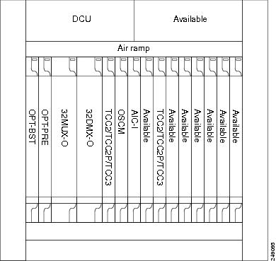
Figure 12-2 shows an example of a terminal configuration with a 40-WSS-C card installed.
Figure 12-2 Terminal Node Configuration with 40-WSS-C Cards Installed
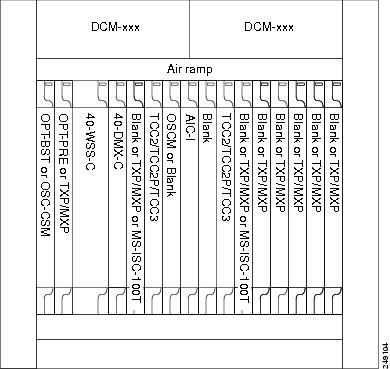
Figure 12-3 shows an example of a terminal configuration with a 40-MUX-C card installed.
Figure 12-3 Terminal Node with 40-MUX-C Cards Installed
Figure 12-4 shows an example of a terminal configuration with a 40-SMR1-C card installed.
Figure 12-4 Terminal Node with 40-SMR1-C Card Installed - Cisco ONS 15454 and Cisco ONS 15454 M6

Figure 12-5 shows an example of a terminal configuration with 40-SMR1-C and booster amplifier cards installed.
Figure 12-5 Terminal Node with 40-SMR1-C and Booster Amplifier Cards Installed - Cisco ONS 15454 and Cisco ONS 15454 M6
Note When you use the 40-SMR1-C card along with a booster amplifier, the OSCM card must be connected to the booster amplifier.
Figure 12-6 shows an example of a terminal configuration with a 40-SMR2-C card installed.
Figure 12-6 Terminal Node with 40-SMR2-C Card Installed - Cisco ONS 15454 and Cisco ONS 15454 M6
Figure 12-7 shows an example of a 80-channel terminal configuration with RAMAN-CTP and RAMAN-COP cards installed.
Figure 12-7 80-Channel Terminal Node with RAMAN-CTP and RAMAN-COP Cards Installed - Cisco ONS 15454 M6
12.1.2 OADM Node
An OADM node is a single ONS 15454 node equipped with cards installed on both sides and at least one AD-xC-xx.x (or FLD-4-xx.x) card or one AD-xB-xx.x card (plus their related 4MD-xx.x cards) and two TCC2/TCC2P/TCC3/TNC/TNCE/TSC/TSCE cards. This configuration supports 32 channels. In an OADM node, channels can be added or dropped independently from each direction and then passed through the reflected bands of all OADMs in the DWDM node (called express path). They can also be passed through one OADM card to another OADM card without using a TDM ITU-T line card (called optical pass-through) if an external patchcord is installed.
Unlike express path, an optical pass-through channel can be converted later to an add/drop channel in an altered ring without affecting another channel. OADM amplifier placement and required card placement is determined by the Cisco TransportPlanner tool or your site plan.
OADM nodes can be amplified or passive. In amplified OADMs, booster and preamplifier cards are installed on bode sides of the node. Figure 12-8 shows an example of an amplified OADM node configuration. In addition, OADM nodes can be asymmetric. Amplifiers may be installed in one side, but not the other. Or preamplifiers may be installed in one side, and a booster in the other.
Figure 12-8 Amplified OADM Node Configuration Example
Figure 12-9 shows an example of the channel flow on the amplified OADM node. Since the 32-wavelength plan is based on eight bands (each band contains four channels), optical adding and dropping can be performed at the band level and/or at the channel level (meaning individual channels can be dropped).
Figure 12-9 Amplified OADM Node Channel Flow Example
Specifying the number of circuits that are currently present on an amplifier that is receiving the power directly from the15216-FLD-4 passive units (in case of an OADM node with FLD-4 cards and when an APC domain is in passive state) enables an accurate calculation of the power gain on the amplified port. This also ensures that the amplifier works effectively when the number of circuits is lesser than the actual circuits provisioned (where APC does not run in those domains.
To provision the number of active circuits, in CTC go to the card view, click > Maintenance > Manual Gain Calc tabs and enter the number of circuits currently active and then click Apply . Changing the value forces the system to recalculate the gain in order to obtain a more suitable output power.
You can manually provision the number of active circuits only if one of the following conditions are satisfied:
12.1.3 ROADM Node
A ROADM node adds and drops wavelengths without changing the physical fiber connections. A ROADM node is equipped with two TCC2/TCC2P/TCC3/TNC/TNCE/TSC/TSCE cards and one of the following combinations:
- Two 32WSS cards and either, two 32DMX or 32DMX-O cards
- Two 40-WSS-C or 40-WSS-CE cards and either, two 40-DMX-C or 40-DMX-CE cards
- Two 40-SMR1-C cards and two 15216-MD-40-ODD, 15216-EF-40-ODD, or 15216-MD-48-ODD (ONS 15216 40 or 48-channel mux/demux) patch panels
- Two 40-SMR1-C cards, two line amplifiers (OPT-BST, OPT-BST-E, OPT-AMP-C, or OPT-AMP-17C cards), two OPT-RAMP-C or OPT-RAMP-CE cards, and two 15216-MD-40-ODD, 15216-EF-40-ODD, or 15216-MD-48-ODD patch panels
- Two 40-SMR2-C cards and two 15216-MD-40-ODD, 15216-EF-40-ODD, or 15216-MD-48-ODD patch panels
- Two 80-WXC-C cards and two 15216-MD-40-ODD, 15216-EF-40-ODD, 15216-MD-48-ODD, 15216-MD-40-EVEN, 15216-EF-40-EVEN, or 15216-MD-48-EVEN patch panels
Note Although it is recommended that you use the 15216-MD-40-ODD, 15216-EF-40-ODD, or 15216-MD-48-ODD patch panel along with the 40-SMR1-C and 40-SMR2-C cards, you can alternatively use the 40-MUX-C and 40-DMX-C cards instead of the 15216-MD-40-ODD, 15216-EF-40-ODD, or 15216-MD-48-ODD patch panel.
Transponders (TXPs) and muxponders (MXPs) can be installed in Slots 6 and 12 and, if amplification is not used, in any open slot.
Note Although not required, 32DMX-O can be used in a ROADM node. Cisco TransportPlanner automatically chooses the demultiplexer card that is best for the ROADM node based on the network requirements.
Figure 12-10 shows an example of an amplified ROADM node configuration with 32DMX cards installed.
Figure 12-10 ROADM Node with 32DMX Cards Installed
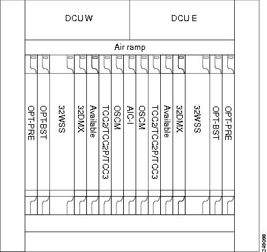
Figure 12-11 shows an example of an amplified ROADM node configuration with 40-WSS-C cards installed.
Figure 12-11 ROADM Node with 40-WSS-C Cards Installed
Figure 12-12 shows an example of a ROADM node with 40-SMR1-C cards installed.
Figure 12-12 ROADM Node with 40-SMR1-C Cards Installed - Cisco ONS 15454 and Cisco ONS 15454 M6

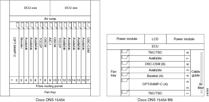
Figure 12-13 shows an example of a ROADM node with 40-SMR1-C and booster amplifier cards installed.
Figure 12-13 ROADM Node with 40-SMR1-C and Booster Amplifier Cards Installed - Cisco ONS 15454 and Cisco ONS 15454 M6
Note When you use the 40-SMR1-C card along with a booster amplifier, the OSCM card must be connected to the booster amplifier.
Figure 12-14 shows an example of a ROADM node with 40-SMR1-C and OPT-RAMP-C cards installed.
Figure 12-14 ROADM Node with 40-SMR1-C and OPT-RAMP-C Cards Installed
Figure 12-15 shows an example of a ROADM node with 40-SMR2-C cards installed.
Figure 12-15 ROADM Node with 40-SMR2-C Cards Installed - Cisco ONS 15454 and Cisco ONS 15454 M6
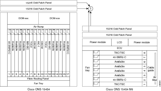
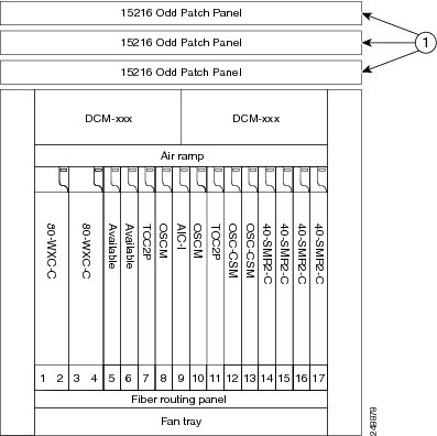
Figure 12-16 shows an example of a colored two-degree ROADM node using 80-WXC-C cards with booster and preamplifier cards. The 80-WXC-C cards are inserted in Slots 3 and 14, and function in the bidirectional mode.
Figure 12-16 Colored Two-Degree ROADM Node with 80-WXC-C, Booster, and Preamplifier Cards

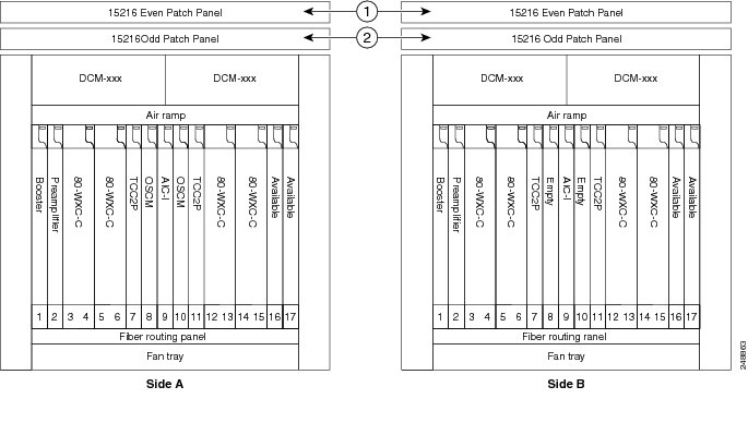
Figure 12-17 shows an example of an ONS 15454 M6 80-channel colored two-degree ROADM node.
Figure 12-17 ONS 15454 M6 80-Channel Colored Two-degree ROADM Node
Figure 12-18 shows the layout of an 80-channel n-degree ROADM node with omni-directional side.
Figure 12-18 80-Channel n-degree ROADM node with Omni-directional Side
Figure 12-19 shows the layout of an ONS 15454 M6 80-channel n-degree ROADM node with omni-directional side.
Figure 12-19 ONS 15454 M6 80-Channel n-degree ROADM Node with Omni-directional Side
Figure 12-20 shows the layout of a 40-channel n-degree ROADM node with a 40-WXC-C based colorless side.
Figure 12-20 40-Channel n-degree ROADM Node with 40-WXC-C Based Colorless Side
The 80-WXC-C cards are connected to the ADD/DROP ports of the 40-WXC-C card and function as colorless multiplexer and demultiplexer units.
Figure 12-21 shows the layout of a 40-channel four-degree ROADM node with a 40-SMR2-C based colorless side.
Figure 12-21 40-Channel Four-degree ROADM Node with 40-SMR2-C Based Colorless Side
The 80WXC-C (multiplexer) card is inserted in Slot 3 and the 80-WXC-C (demultiplexer) card is inserted in Slot 5. The 80-WXC-C cards are connected to the ADD/DROP ports of the 40-SMR2-C card and function as the colorless multiplexer and demultiplexer units.
Figure 12-22 shows the layout for an 80-channel colorless ROADM node.
Figure 12-22 80-Channel Colorless ROADM Node
An 80 channel colorless two-degree ROADM node requires the following cards: 80-WXC-C, 15216-MD-40-ODD, 15216-EF-40-ODD, 15216-MD-48-ODD, 15216-MD-40-EVEN, 15216-EF-40-EVEN, 15216-MD-48-EVEN, preamplifiers, and boosters.
The 80-WXC-C cards can be used at two levels; level1 (L1) and level2 (L2).
The L1 80WXC-C (multiplexer) card is inserted in Slot 3 and the L1 80-WXC-C (demultiplexer) card is inserted in Slot 5. The L2 80WXC-C (multiplexer) card is inserted in Slot 12 and the L2 80-WXC-C (demultiplexer) card is inserted in Slot 14.
Figure 12-23 shows an example of the optical signal flow in an 80-channel colorless two-degree ROADM node from Side A to Side B using 80-WXC-C cards. The optical signal flow from Side B to Side A follows an identical path.
Figure 12-23 80-Channel Colorless Two-degree ROADM Node
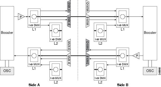
The booster on Side A receives the composite optical signal. It separates the optical service channel from the optical payload and sends the payload to the preamplifier on Side A. |
|
The preamplifier compensates for chromatic dispersion, amplifies the optical payload and sends it to the L1 80-WXC-C card (demultiplexer). |
|
Up to eight colorless ports are available on the L1 80-WXC-C card if no colored wavelength is terminated. In Figure 12-23, two EAD ports are connected to 40-DMX-C or 40-DMX-CE cards, 15216-MD-40-ODD, 15216-EF-40-ODD, 15216-MD-48-ODD, 15216-MD-40-EVEN, 15216-EF-40-EVEN, or 15216-MD-48-EVEN units where the colored odd and even wavelengths are dropped. The express wavelengths are sent to the L1 80-WXC-C card (multiplexer) on Side B where the wavelengths are multiplexed with other colored or colorless wavelengths. |
|
The L1-80-WXC-C card on Side B sends the composite signal to the booster on Side B. |
|
The booster on Side B receives the composite optical signal, adds the optical service channel to the optical payload and sends it to the transmission line. |
|
It is possible to configure more colorless ports by cascading the 80-WXC-C cards at two levels. For example, to get 14 colorless ports connect one of the EAD ports of the L1 80-WXC-C card to another 80-WXC-C cards at level 2. There are five colorless ports on the L1 80-WXC-C card and nine colorless ports on the L2 80-WXC-C card. To achieve an 80 channel colorless configuration, connect nine L2 80-WXC-C cards to the nine EAD ports of the L1 80-WXC-C card. |
Figure 12-24 shows the layout for an 80-channel colorless ROADM node with OPT-RAMP-C cards.
Figure 12-24 80-Channel Colorless ROADM Node with OPT-RAMP-C Card
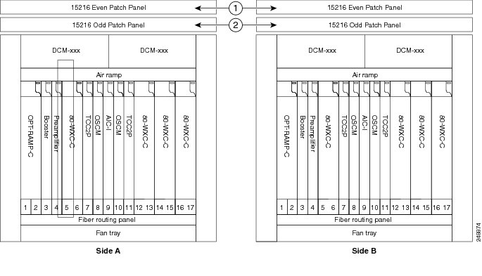
Figure 12-25 shows an example of an ONS 15454 M6 80-channel two degree colorless ROADM node.
Figure 12-25 ONS 15454 M6 80-Channel Two-degree Colorless ROADM Node
The L1 80WXC-C (multiplexer) card is inserted in Slot 4 and the L1 80-WXC-C (demultiplexer) is inserted in Slot 6. The L2 80WXC-C (multiplexer) card is inserted in Slot 2 and the L2 80-WXC-C (demultiplexer) is inserted in Slot 4.
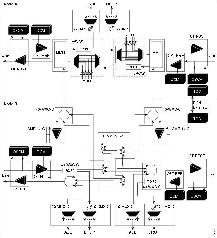
Figure 12-27 shows an example of a ROADM optical signal flow from Side A to Side B using the 32WSS or 40-WSS-C cards. The optical signal flow from Side B to Side A follows an identical path through the Side B OSC-CSM and 32WSS or 40-WSS-C cards. In this example, OSC-CSM cards are installed, hence OPT-BSTs are not needed.
Figure 12-26 shows an example of an ONS 15454 M6 80-channel ROADM node with RAMAN-CTP cards installed.
Figure 12-26 Cisco ONS 15454 M6 80-Channel ROADM Node Using RAMAN-CTP Cards
Figure 12-27 ROADM Optical Signal Flow Example Using 32WSS or 40-WSS-C Card
Figure 12-28 shows an example of an ROADM optical signal flow from Side A to Side B using the 40-SMR1-C card. The optical signal flow from Side B to Side A follows an identical path through the Side B booster and 40-SMR1-C card.
Figure 12-28 ROADM Optical Signal Flow Example Using 40-SMR1-C Card
12.1.4 Hub Node
A hub node is a single ONS 15454 node equipped with two TCC2/TCC2P/TCC3/TNC/TNCE/TSC/TSCE cards and one of the following combinations:
- Two 32MUX-O cards and two 32DMX-O or 32DMX cards
- Two 32WSS cards and two 32DMX or 32DMX-O cards
- Two 40-WSS-C or 40-WSS-CE cards and two 40-DMX-C or 40DMX-CE cards
- Two 40-SMR1-C and two 15216-MD-40-ODD, 15216-EF-40-ODD, or 15216-MD-48-ODD (ONS 15216 40 or 48-channel mux/demux patch panel)
- Two 40-SMR2-C and two 15216-MD-40-ODD, 15216-EF-40-ODD, or 15216-MD-48-ODD
Note Although it is recommended that you use the 15216-MD-40-ODD, 15216-EF-40-ODD, or 15216-MD-48-ODD patch panel along with the 40-SMR1-C and 40-SMR2-C cards, you can alternatively use the 40-MUX-C and 40-DMX-C cards instead of the 15216-MD-40-ODD, 15216-EF-40-ODD, or 15216-MD-48-ODD patch panel.
Note The configuration for a hub node using 40-SMR1-C or 40-SMR2-C cards is identical to the ROADM node, except that there is no patchcord connecting the two 40-SMR1-C or 40-SMR2-C cards. For more details on the ROADM node configuration, see the “ROADM Node” section.
Note The 32WSS/40-WSS-C/40-WSS-CE and 32DMX/32DMX-L/40-DMX-C/ 40-DMX-CE cards are normally installed in ROADM nodes, but they can also be installed in hub and terminal nodes. If the cards are installed in a hub node, the 32WSS/32WSS-L/ 40-WSS-C/40-WSS-CE express ports (EXP RX and EXP TX) are not cabled.
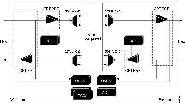
A dispersion compensation unit (DCU) can also be added, if necessary. Figure 12-29 shows a hub node configuration with 32MUX-O and 32DMX-O cards installed.
Figure 12-29 Hub Node Configuration Example with 32-Channel C-Band Cards
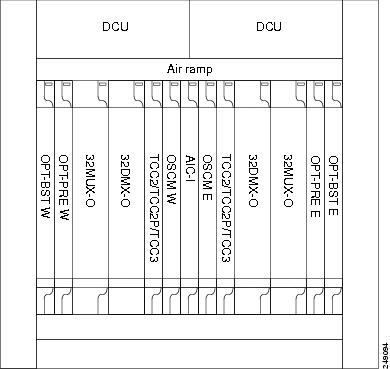
Figure 12-30 shows a 40-channel hub node configuration with 40-WSS-C cards installed.
Figure 12-30 Hub Node Configuration Example with 40-WSS-C Cards

Figure 12-31 shows the channel flow for a hub node. Up to 32 channels from the client ports are multiplexed and equalized onto one fiber. Then, multiplexed channels are transmitted to the OPT-BST amplifier. The OPT-BST output is combined with an output signal from the OSCM card and transmitted to the other side.
Received signals are divided between the OSCM card and an OPT-PRE card. Dispersion compensation is applied to the signal received by the OPT-PRE amplifier, and it is then sent to the 32DMX-O card, which demultiplexes and attenuates the input signal.
Figure 12-31 Hub Node Channel Flow Example
12.1.5 Anti-ASE Node
In a mesh ring network, the ONS 15454 requires a node configuration that prevents ASE accumulation and lasing. An anti-ASE node can be created by configuring a hub node or an OADM node with some modifications. No channels can travel through the express path, but they can be demultiplexed and dropped at the channel level on one side and added and multiplexed on the other side.
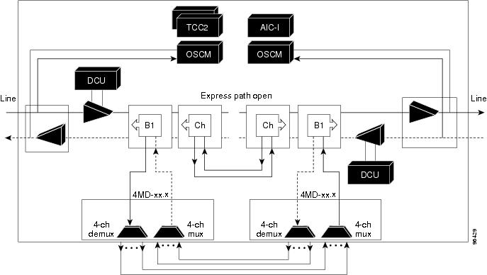
The hub node is the preferred node configuration when some channels are connected in pass-through mode. For rings that require a limited number of channels, combine AD-xB-xx.x and 4MD-xx.x cards, or cascade AD-xC-xx.x cards. See Figure 12-9.
Figure 12-32 shows an anti-ASE node that uses all wavelengths in the pass-through mode. Use Cisco TransportPlanner to determine the best configuration for anti-ASE nodes.
Figure 12-32 Anti-ASE Node Channel Flow Example
12.1.6 Line Amplifier Node
A line amplifier node is a single ONS 15454 node that is used to amplify the optical signal in long spans. The line amplifier node can be equipped with one of the following sets of cards:
- Two OPT-PRE cards, two OPT-BST cards, and two OSCM cards
- Two OPT-PRE cards and two OSC-CSM cards
- Two OPT-AMP-17-C cards and two OSCM cards
- Two OPT-AMP-C cards and two OSCM cards
Attenuators might also be required between each preamplifier and OPT-BST amplifier to match the optical input power value and to maintain the amplifier gain tilt value.
Two OSCM cards are connected to the OPT-BST cards to multiplex the OSC signal with the pass-though channels. If the node does not contain a booster card, OSC-CSM cards must be installed instead of OSCM cards. Figure 12-33 shows an example of a line amplifier node configuration using OPT-BST, OPT-PRE, and OSCM cards.
Figure 12-33 Line Amplifier Node Configuration Example - Cisco ONS 15454 M6 and Cisco ONS 15454 M2
The line amplifier can be equipped with OPT-RAMP-C or OPT-RAMP-CE cards to achieve in fiber amplification. Figure 12-34 shows an example of a line amplifier node with Raman amplification using OPT-RAMP-C cards.
Figure 12-34 Line Amplifier Node with OPT-RAMP-C Cards

A node layout equipped with OPT-RAMP-C or OPT-RAMP-CE cards without post-amplifiers is used when post-amplification of the optical signal is not required.
This layout is used in the following scenarios:
There are three node layouts without post-amplifiers:
1. Line amplifier node equipped with OPT-RAMP-C or OPT-RAMP-CE cards on Side A and Side B.
2. Line amplifier node equipped with OPT-RAMP-C or OPT-RAMP-CE and booster cards on Side A and OPT-RAMP-C or OPT-RAMP-CE cards on Side B and vice-versa.
3. Line amplifier node equipped with OPT-RAMP-C or OPT-RAMP-CE and booster cards on Side A and OSC-CSM cards on Side B and vice-versa.
Figure 12-35 shows an example of a line amplifier node with OPT-RAMP-C cards on Side A and Side B.
Figure 12-35 Line Amplifier Node with OPT-RAMP-C Cards on Sides A and B
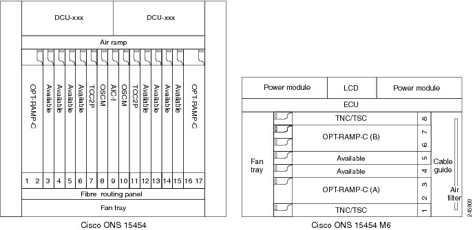
Figure 12-36 shows an example of a line amplifier node with a standard Raman configuration (OPT-RAMP-C or OPT-RAMP-CE and booster cards) on Side A and a Raman only configuration (OPT-RAMP-C or OPT-RAMP-CE cards) on Side B.
Figure 12-36 Line Amplifier Node with OPT-RAMP-C and Booster Cards (Side A) and OPT-RAMP-C Cards (Side B)

Figure 12-37 shows an example of a line amplifier node with a standard Raman configuration (OPT-RAMP-C or OPT-RAMP-CE and booster cards) on Side A and an OSC-CSM configuration on Side B.
Figure 12-37 Line Amplifier Node with OPT-RAMP-C and Booster Cards (Side A) and OSC-CSM Cards (Side B)
12.1.7 OSC Regeneration Node
The OSC regeneration node is added to the DWDM networks for two purposes:
- To electrically regenerate the OSC channel whenever the span links are 37 dB or longer and payload amplification and add/drop capabilities are not present. Cisco TransportPlanner places an OSC regeneration node in spans longer than 37 dB. The span between the OSC regeneration node and the next DWDM network site cannot be longer than 31 dB.
- To add data communications network (DCN) capability wherever needed within the network.
OSC regeneration nodes require two OSC-CSM cards, as shown in Figure 12-38. The cards are installed in each side of the shelf.
Figure 12-38 OSC Regeneration Line Node Configuration Example - Cisco ONS 15454, Cisco ONS 15454 M6, and Cisco ONS 15454 M2
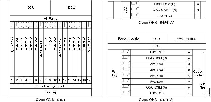
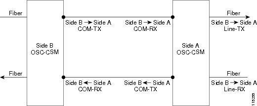
Figure 12-39 shows the OSC regeneration line node signal flow.
Figure 12-39 OSC Regeneration Line Node Flow
12.2 Supported Node Configurations for OPT-RAMP-C and OPT-RAMP-CE Cards
The OPT-RAMP-C and OPT-RAMP-CE cards can be equipped in the following network element type configurations:
– C-band terminal site with 32-MUX-O and 32-DMX-O cards
– C-band hub node with 32-MUX-O and 32-DMX-O cards
– C-band 32-channel reconfigurable OADM (ROADM)
– C-band terminal site using a 32-WSS and 32-DMX cards
– C-band flexible terminal site using AD-xC cards
– C-band hub node using a 32-WSS and 32-DMX cards
– C-band terminal site using a 40-WSS-C and 40-DMX-C cards
– C-band terminal site using 40-MUX-C and 40-DMX-C cards
– C-band hub node using a 40-WSS-C and 40-DMX-C cards
– C-band up to 4 degree mesh node
– C-band up to 8 degree mesh node
– C-band multiring/mesh with MMU node
– C-band 4 degree multiring/mesh node (MMU based)
– C-band 64-channel terminal site
– C-band 72-channel terminal site
– C-band 80-channel terminal site
– C-band 64-channel ROADM site
– C-band 72-channel ROADM site
– C-band 80-channel ROADM site
The following amplifier cards are defined as booster or preamplifiers:
Note When the booster is not needed, it must be replaced with an OSC-CSM card.
12.2.1 OPT-RAMP-C or OPT-RAMP-CE Card in an Add/Drop Node
When the OPT-RAMP-C or OPT-RAMP-CE card is equipped in an add/drop node, the booster amplifier is mandatory and cannot be replaced by an OSC-CSM card. The preamplifier is an OPT-BST, OPT-BST-E, or OPT-AMP-C card, and must be cabled as an unidirectional card. Note that the COM-TX and LINE-RX ports must not be used for any other connections. If a single module ROADM 40-SMR-1-C is used as an add/drop card, a preamplifier is not required. If a single module ROADM 40-SMR-2-C is used as an add/drop card, both the preamplifier and booster are not required.
Figure 12-40 shows the OPT-RAMP-C or OPT-RAMP-CE card in an add/drop node.
Figure 12-40 OPT-RAMP-C or OPT-RAMP-CE Card in an Add/Drop Node
When required, a DCN extension can be used on A/D Side (i) in Figure 12-40.
Side (i) in Figure 12-40 can be equipped with the following cards:
12.2.2 OPT-RAMP-C or OPT-RAMP-CE Card in a Line Site Node with Booster Amplification
The OPT-RAMP-C or OPT-RAMP-CE card can be equipped in a line site node with a booster amplifier in the following configurations:
- OPT-BST and OPT-BST-E can be used as booster in a line site node with OPT-RAMP-C or OPT-RAMP-CE. The booster cards need to be cabled as bidirectional units. Figure 12-41 shows the OPT-RAMP-C or OPT-RAMP-CE card in a line site configuration.
Figure 12-41 OPT-RAMP-C Card or OPT-RAMP-CE Card in a Line Site Configuration
- The OPT-AMP-C can be used as a booster in a line site node with OPT-RAMP-C or OPT-RAMP-CE and needs to be cabled as a bidirectional unit. An additional DCU unit can be equipped between the OPT-AMP-C DC ports. Figure 12-42 shows a line site configured with OPT-AMP-C card and an additional DCU unit.
Figure 12-42 Line Site Configured with OPT-AMP-C
- A line site can be configured with OPT-RAMP-C or OPT-RAMP-CE card on one side only. Figure 12-43 shows the line site configured with OPT-RAMP-C or OPT-RAMP-CE on side A only. The booster is configured on side B.
Figure 12-43 Line Site with OPT-RAMP-C or OPT-RAMP-CE On One Side
In all configurations, the booster amplifier facing the OPT-RAMP-C or OPT-RAMP-CE card is mandatory for safety reasons.
12.2.3 OPT-RAMP-C or OPT-RAMP-CE Card in a Line Site Node Without Post - Amplification
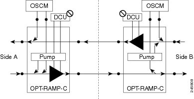
The OPT-RAMP-C or OPT-RAMP-CE card can be equipped in a line site node in the following configurations:
- A symmetric Raman configuration without post-amplifiers with an OPT-RAMP-C or OPT-RAMP-CE card on Side A and Side B in a line site node (see Figure 12-44). In this configuration, the OPT-RAMP-C or OPT-RAMP-CE cards do not support DCU units.
Figure 12-44 Symmetric Raman Configuration Without Post-Amplifiers
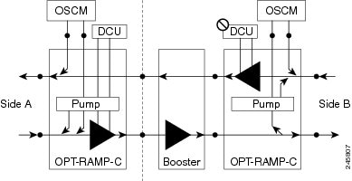
- An asymmetric configuration of a line site node where Side A is a standard Raman configuration equipped with OPT-RAMP-C or OPT-RAMP-CE and booster cards and Side B is a Raman configuration without post-amplifiers and is equipped with OPT-RAMP-C or OPT-RAMP-CE cards (see Figure 12-45). Side B does not support DCU units.
Figure 12-45 Asymmetric Configuration With Standard Raman on Side A and Raman Without Post-Amplifier on Side B
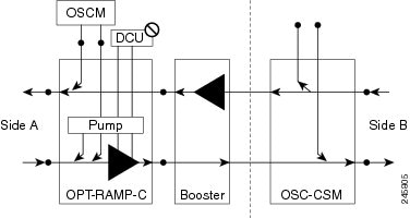
- An asymmetric configuration of a line site node where Side A is a Raman configuration without post-amplifier equipped with OPT-RAMP-C or OPT-RAMP-CE cards (without DCU units) and Side B is configured with OSC-CSM cards (see Figure 12-46).
Figure 12-46 Asymmetric configuration With One Side Configured as Raman Without Post-Amplifier
12.3 Supported Node Configurations for PSM Card
The PSM card supports the following node configurations:
12.3.1 Channel Protection
In a channel protection configuration, the PSM card is used in conjunction with a TXP/MXP card. The PSM card in a channel protection configuration can be used in any site apart from a terminal site.
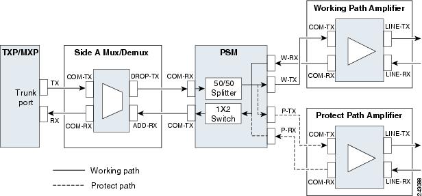
Figure 12-47 shows the DWDM functional view of a PSM card in channel protection configuration.
Figure 12-47 PSM Channel Protection Configuration
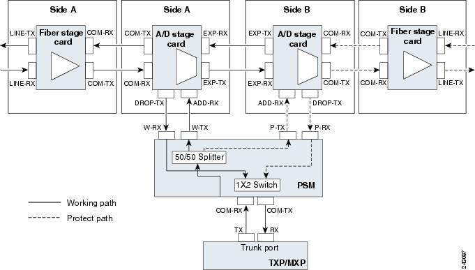
In this configuration, the COM-RX and COM-TX ports of the PSM card are connected to the TXP/MXP trunk ports. This configuration is applicable to an n -degree MSTP node, for example, a two-degree ROADM, an n -degree ROADM, or an OADM node. The example block diagram shows a two-degree node with Side A and Side B as the two sides. The Side A and Side B fiber-stage block can be DWDM cards that are used to amplify transmitted or received signal (see the “Fiber Stage” section for the list of cards). The Side A and Side B add/drop stage block can be DWDM cards that can add and drop traffic (see the “A/D Stage” section for the list of cards).
In the transmit direction, the traffic originating from a TXP/MXP trunk port is split by the PSM card on to the W-TX and P-TX ports. The W-TX and P-TX ports are connected to the ADD-RX ports of the add/drop stage cards in Side A and Side B respectively. The add/drop stage cards multiplex traffic on Side A and Side B line ports that become the working and protect paths respectively.
In the receive direction, the W-RX and P-RX ports of the PSM card are connected to the DROP-TX ports of the add/drop stage cards on Side A and Side B respectively. The add/drop stage cards demultiplex traffic received from Side A and Side B line ports that are the working and protect paths respectively. The PSM card selects one of the two input signals on the W-RX and P-RX ports to be transmitted to the COM-RX port of the PSM card.
Note All traffic multiplexed or demultiplexed by the two add/drop stage cards is not protected.
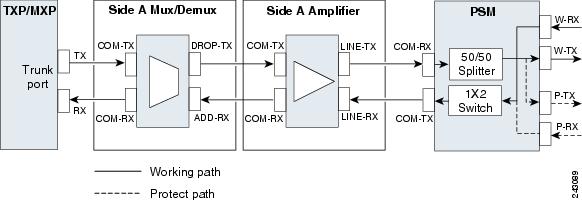
12.3.2 Multiplex Section Protection
The PSM card performs multiplex section protection when connected between a multiplexer/demultiplexer card in a terminal site. The multiplexer/demultiplexer stage can be built using WSS and DMX or 40MUX and 40DMX cards. The terminal sites can be 50/100 Ghz band. The number of supported channels can therefore be 32/40 or 72/80.
Figure 12-48 shows the block diagram of a PSM card in multiplex section protection configuration.
Figure 12-48 PSM Multiplex Section Protection Configuration
In the transmit direction, the traffic originating from a TXP trunk port is multiplexed by the Side A multiplexer. The PSM card splits traffic on to the W-TX and P-TX ports, which are independently amplified by two separated booster amplifiers.
In the receive direction, the signal on the line ports is preamplified by two separate preamplifiers and the PSM card selects one of the two input signals on the W-RX and P-RX ports to be transmitted to the COM-RX port of the PSM card. The received signal is then demultiplexed to a TXP card.
The presence of a booster amplifier is not mandatory. However, if a DCN extension is used, the W-TX and P-TX ports of the PSM card can be connected directly to the line. The presence of a preamplifier is also not mandatory.
Note The PSM card cannot be used with Raman amplification in a line protection or section protection configuration.
12.3.3 Line Protection
In a line protection configuration, the working and protect ports of the PSM card are connected directly to the external line. This configuration is applicable to any MSTP node that is configured as a terminal site. The multiplexer/demultiplexer stage can be built using WSS and DMX, 40MUX and 40DMX, 40-SMR1-C and 15216-MD-40-ODD, 15216-EF-40-ODD, or 15216-MD-48-ODD, or 40-SMR2-C and 15216-MD-40-ODD, 15216-EF-40-ODD, or 15216-MD-48-ODD units. The terminal sites can be 50/100 Ghz band. The number of supported channels can therefore be 32/40 or 72/80.
Figure 12-49 shows the block diagram of a PSM card in line protection configuration.
Figure 12-49 PSM Line Protection Configuration
In the transmit direction, the traffic originating from a transponder trunk port is multiplexed by the Side A multiplexer and amplified by a booster amplifier. The Line-TX port of the amplifier is connected to the COM-RX port of the PSM card. The PSM card splits traffic received on the COM-RX port on to the W-TX and P-TX ports, which form the working and protect paths.
In the receive direction, the PSM card selects one of the two input signals on the W-RX and P-RX ports to be transmitted to the COM-RX port of the PSM card. The received signal is then preamplified and demultiplexed to the TXP card.
The presence of a booster amplifier is not mandatory. However, if a DCN extension is used, the COM-RX port of the PSM card is connected to the multiplex section. The presence of a preamplifier is also not mandatory; the COM-TX port of the PSM card can be connected to the demultiplexer.
Note The PSM card cannot be used with Raman amplification in a line protection or section protection configuration.
12.3.4 Standalone
In a standalone configuration, the PSM card can be equipped in any slot and supports all node configurations. In this configuration, the PSM card provides only basic functionality, such as, protection against a fiber cut, optical safety, and automatic laser shutdown (ALS). It does not provide other functionalities such as, automatic power control (APC), automatic node setup (ANS), network and node alarm correlation, circuit management, and so on.
12.4 Multishelf Node
In a multishelf configuration, the ONS 15454 M6 node or the ONS 15454 DWDM node with TCC3 card as the node controller can manage up to 49 subtending shelves as a single entity. The subtending shelves can be ONS 15454 M6 or ONS 15454 DWDM nodes.
The node controller is the main shelf with the TCC2/TCC2P/TCC3/TNC/TNCE/TSC/TSCE cards running the multishelf functions. Each subtending shelf must be equipped with TCC2/TCC2P/TCC3/TNC/TNCE/TSC/TSCE cards, which run the shelf functions. For internal data exchange between the node controller shelf and subtending shelves, the node controller shelf must be equipped with redundant MS-ISC-100T cards, external connection unit (ECU), or external connection unit2 (ECU2) modules. As an alternative, the Catalyst 2950 or the Catalyst 3560 switch can be used for internal data exchange between the node controller shelf and subtending shelves. It is recommend that you use the MS-ISC-100T cards. If using the Catalyst 2950 or the Catalyst 3560 switch, it is installed on one of the multishelf racks. All subtending shelves must be located in the same site at a maximum distance of 100 meters or 328 feet from the Ethernet switches used to support the communication LAN.
Figure 12-50 shows an example of a multishelf node configuration.
Figure 12-50 Multishelf Node Configuration
A multishelf node has a single public IP address for all client interfaces (Cisco Transport Controller [CTC], Transaction Language One [TL1], Simple Network Management Protocol [SNMP], and HTTP); a client can only connect to the node controller shelf, not to the subtending shelves. The user interface and subtending shelves are connected to a patch panel using straight-through (CAT-5) LAN cables.
The node controller shelf has the following functions:
- IP packet routing and network topology discovery at the node controller level.
- Open Shortest Path First (OSPF) centralized on the node controller shelf.
The subtending shelves have the following functions:
- Overhead circuits are not routed within a multishelf node but are managed at the subtending controller shelf only. To use overhead bytes, the AIC-I must be installed on the subtending shelf where it is terminated.
- Each subtending shelf will act as a single shelf node that can be used as a timing source line, TCC/TCC2P/TCC3/TNC/TNCE/TSC/TSCE clock, or building integrated timing supply (BITS) source line.
12.4.1 Multishelf Node Layout
Multishelf configurations are configured by Cisco TransportPlanner and are automatically discovered by the CTC software. In a typical multishelf installation, all optical units are equipped on the node controller shelf and TXP/MXP cards are equipped in the aggregated subtended shelves. In addition, all empty slots in the node controller shelf can be equipped with TXP/MXP cards. In a DWDM mesh network, up to eight optical sides can be configured with client and optical cards installed in different shelves to support mesh and ring-protected signal output.
Note When a DWDM ring or network has to be managed through a Telcordia operations support system (OSS), every node in the network must be set up as multi-shelf. OLA sites and nodes with one shelf must be set up as “multi-shelf stand-alone” to avoid the use of LAN switches.
12.4.2 DCC/GCC/OSC Terminations
A multishelf node provides the same communication channels as a single-shelf node:
- OSC links terminate on OSCM/OSC-CSM cards. Two links are required between each ONS 15454 node. An OSC link between two nodes cannot be substituted by an equivalent generic communications channel/data communications channel (GCC/DCC) link terminated on the same pair of nodes. OSC links are mandatory and they can be used to connect a node to a gateway network element (GNE).
- GCC/DCC links terminate on TXP/MXP cards.
The maximum number of DCC/GCC/OSC terminations that are supported in a multishelf node is 48.
Note Optical Service Channel can be created on the OC3 port of the TNC and TNCE cards.
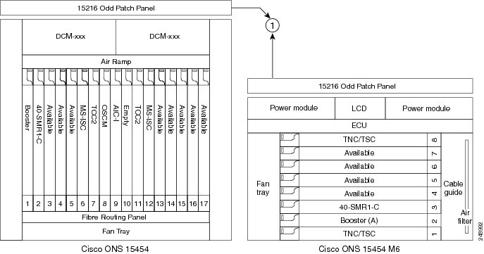
12.5 Connecting Passive Modules to a ONS 15454 M2 or ONS 15454 M6 Node
The non-volatile flash memory of the passive optical modules store inventory and insertion loss (IL) data of the optical paths. The stored data can be retrieved through the USB port of the passive optical module by connecting it to the transport node controller card (TNC) of the Cisco ONS 15454 M2 or Cisco ONS 15454 M6 shelf assembly.
You can connect the following passive modules to an USB port of the Cisco ONS 15454 M2 or Cisco ONS 15454 M6 node:
- 15216-FLD-4
- 15216-MD-40-EVEN
- 15216-EF-40-EVEN
- 15216-MD-48-EVEN
- 15216-MD-40-ODD
- 15216-EF-40-ODD
- 15216-MD-48-ODD
- 15216-MD-ID-50
- 15216-MD-48-CM
- 15216-FBGDCU
For the related procedure, see G319 Connect a Passive Module to the Cisco ONS 15454 M2 or Cisco ONS 15454 M6 Node.
12.6 Optical Sides
From a topological point of view, all DWDM units equipped in an MSTP node belongs to a side. A side can be identified by a letter (A, B, C, D, E, F, G, or H), or by the ports (called as side line ports, see Side Line Ports) that are physically connected to the spans. An MSTP node can be connected to a maximum of 8 different spans. Each side identifies one of the spans the MSTP node is connected to.
Note Side A and Side B replace “west” and “east” when referring to the two sides of the ONS 15454 shelf. Side A refers to Slots 1 through 6 (formerly “west”), and Side B refers to Slots 12 through 17 (formerly “east”). The line direction port parameter, East-to-West and West-to-East, has been removed.
Sides are viewed and managed from the Provisioning > WDM-ANS > Optical Sides tab in CTC.
12.6.1 Optical Side Stages
All MSTP nodes can be modelled according to Figure 12-51.
Figure 12-51 Interconnecting Sides Conceptual View
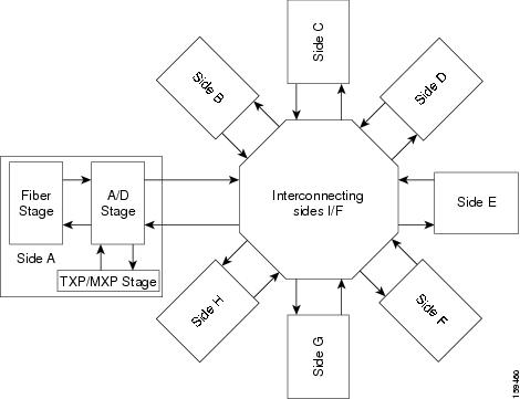
According to Figure 12-51, each MSTP node side includes DWDM units that can be conceptually divided into three stages.
12.6.1.1 Fiber Stage
The fiber stage includes DWDM cards that are used to amplify transmitted or received signals and cards that are used to add optical supervision channels. The fiber stage cards are:
– OPT-AMP-C, when provisioned in OPT-LINE (booster amplifier) mode
– OPT-AMP-L, when provisioned in OPT-LINE (booster amplifier) mode
– OPT-AMP-17-C, when provisioned in OPT-LINE (booster amplifier) mode
– OPT-AMP-C, when provisioned in OPT-PRE (preamplifier) mode
– OPT-AMP-L, when provisioned in OPT-PRE (preamplifier) mode
– OPT-AMP-17-C, when provisioned in OPT-PRE (preamplifier) mode
Table 12-1 shows the commonly deployed fiber stage layouts supported by DWDM mesh nodes. In the table, OPT-BST includes the OPT-BST, OPT-BST-E, and OPT-BST-L cards. OPT-AMP includes the OPT-AMP-L and OPT-AMP-17-C cards configured in either OPT-PRE or OPT-LINE mode.
Note In the table, L and C suffix is not reported because C-band and L-band amplifiers cannot be mixed in the same layout.
12.6.1.2 A/D Stage
The A/D stage includes DWDM cards that can add and drop traffic. The A/D stage is divided into three node types:
- Mesh nodes—ONS 15454 nodes configured in multishelf mode can connect to eight different sides. For more detail on mesh node, see Configuring Mesh DWDM Networks.
- Legacy—Half of a ROADM node or an OADM node with cascaded AD-xB-xx-x or AD-xC-xx.x cards
- Non-A/D—A line node or a side that does not have A/D capability is included in the A/D stage
Stages are built by active cards and patchcords. However, the interconnecting sides are completed by the mesh patch panels (four-degree patch panel or eight-degree patch panel) in mesh nodes, or by patchcords connected to EXP-RX/EXP-TX ports in legacy nodes.
12.6.2 Side Line Ports
Side line ports are ports that are physically connected to the spans. Side line ports can be:
- All ports terminating the fiber stage and physically labeled as LINE, such as ports on the following cards:
– Booster amplifier (OPT-BST, OPT-BST-E, or OPT-BST-L cards, and the OPT-AMP-C, OPT-AMP-L, or OPT-AMP-17-C cards when provisioned in OPT-LINE mode)
– Booster amplifier LINE-RX and LINE-TX ports
– OSC-CSM LINE-RX and LINE-TX ports
– 40-WXC-C COM-RX and COM-TX ports
– MMU EXP-A-RX and EXP-A-TX ports
- All ports that can be physically connected to the external span using DCN terminations in a line node, such as:
– Preamplifier (OPT-PRE card and the OPT-AMP-C, OPT-AMP-L, or OPT-AMP-17-C cards when provisioned in OPT-PRE mode) COM-RX and COM-TX ports
– Booster amplifier COM-TX port
- All ports that can be physically connected to the external span using DCN terminations in a 40-channel MUX/DMX terminal node, such as:
- All ports that can be physically connected to the external span when PSM cards implement line protection:
Note PSM card will support two sides A(w) and A(p).
12.6.3 Optical Side Configurations
You can use the following Side IDs depending on the type of node layout:
- In legacy nodes (that is, a node with no provisioned or installed 40-WXC-C cards), the permissible Side IDs are only A and B.
- In four-degree mesh nodes with four or less 40-WXC-C cards installed, the permissible Side IDs are A, B, C, and D.
- In eight-degree mesh nodes with eight or less 40-WXC-C cards installed, the allowed Side IDs are A, B, C, D, E, F, G, and H.
The system automatically assigns Side IDs when you import the CTP XML configuration file into CTC. You can create a side manually using CTC or TL1 if the following conditions are met:
- You use a permissible side identifier, A through H.
- The shelf contains a TX and an RX side line port (see the “Side Line Ports” section).
- The side line ports are not connected to an internal patchcord.
Note We do not recommend that you manually create or modify ONS 15454 optical sides.
The following tables show examples of how the system automatically assigns Side IDs for common DWDM layouts.
Table 12-2 shows a standard ROADM shelf with Sides A and B provisioned. The shelf is connected to seven shelves containing TXP, MXP, ADM-10G, GE_XP, 10GE_XP, GE_XPE, and 10GE_XPE cards.
Table 12-3 shows a protected ROADM shelf. In this example, Side A and B are Slots 1 through 6 in Shelves 1 and 2. 40-WSS-C/40-WSS-CE/40-DMX-C or 40-WSS-CE/40-DMX-CE cards are installed in Sides A and B. Slots 12 through 17 in Shelves 1 and 2 contain TXP, MXP, ADM-10G, GE_XP, 10GE_XP, GE_XPE, or 10GE_XPE cards.
Table 12-4 shows a four-degree mesh node. Side A is Shelf 1, Slots 1 through 6. Side B and C are Shelf 2, Slots 1 through 6 and 12 through 17, and Side D is Shelf 3, Slots 1 through 6. 40-WXC-C cards in line termination mode are installed in Sides A through D.
Table 12-5 shows a protected four-degree mesh node example. In the example, Sides A through D are assigned to Slots 1 through 6 in Shelves 1 through 4.
Table 12-6 shows a protected four-degree mesh node example. In the example, Sides A through D are assigned to Slots 1 through 4 in Shelves 1 through 4, and TXP, MXP, ADM-10G, GE_XP, 10GE_XP, GE_XPE, or 10GE_XPE cards are installed in Shelves 1 through 4, Slots 12-17, and Shelves 5 through 8, Slots 1 through 6 and 12 through 17.
Table 12-7 shows a four-degree mesh node provisioned as an upgrade. In the example, Sides A through D are assigned to Slots 1 through 4. and 12 through 17 in Shelves 1and 2. 40-WXC-C cards in XC termination mode are installed in Sides A and B, and 40-WXC-C cards in line termination mode are installed in Sides C and D.
Table 12-8 shows an eight-degree mesh node. In the example, Sides A through H are assigned to Slots 1 through 6 in Shelf 1, Slots 1 through 6 and 12 through 17 in Shelves 2 through 4, and Slots 1 through 6 in Shelf 5. 40-WXC-C cards in line termination mode are installed in Sides A through H.
Table 12-9 shows another eight-degree mesh node. In the example, Sides A through H are assigned to Slots 1 through 6 in all shelves (Shelves 1 through 8). 40-WXC-C cards in line termination mode are installed in Sides A through H.
Table 12-10 shows a four-degree mesh node with a user-defined side. Because the software assigns sides consecutively, and because the mesh node is four-degrees, the side assigned to Shelf 5, Slots 1 through 6 is “Unknown.”
12.7 Configuring Mesh DWDM Networks
ONS 15454 shelves can be configured in mesh DWDM networks using the 40-WXC-C or 80-WXC-C wavelength cross-connect cards and four-degree patch panel or eight-degree patch panels. Mesh DWDM networks can also be configured using the 40-SMR2-C cards and the four-degree patch panel.
ONS 15454 DWDM mesh configurations can be up to four degrees (four optical directions) when the four-degree patch panel is installed, and up to eight degrees (eight optical directions) when the eight-degree patch panel is installed. Two mesh node types are available, the line termination mesh node and the cross-connect (XC) termination mesh node.
Note Mesh nodes using the 40-WXC-C or 80-WXC-C card requires multishelf management.
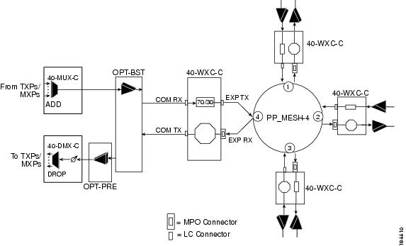
12.7.1 Line Termination Mesh Node Using 40-WXC-C Cards
The line termination mesh node is installed in mesh networks. Line termination mesh nodes can support between one and eight line terminations. Each line direction requires the following cards: 40-WXC-C, 40-MUX-C, 40-DMX-C or 40-DMX-CE, a preamplifier and a booster. Within this configuration, the following substitutions can be used:
- The 40-MUX-C cards can be replaced with 40-WSS-C/40-WSS-CE cards.
- The OPT-BST cards can be replaced with OPT-AMP-17-C (in OPT-BST mode) and/or OPT-BST-E cards.
- The OPT-PRE can be replaced with an OPT-AMP-17-C (in OPT-LINE mode) card.
Each side of the line termination mesh node is connected as follows:
- The 40-WXC-C COM-RX port is connected to the preamplifier output port.
- The 40-WXC-C COM-TX port is connected to the booster amplifier COM-RX port.
- The 40-WXC-C DROP TX port is connected to the 40-DMX-C or 40-DMX-CE COM-RX port.
- The 40-WXC-C ADD-RX port is connected to the 40-MUX-C COM-TX port.
- The 40-WXC-C EXP-TX port is connected to the mesh patch panel.
- The 40-WXC-C EXP-RX port is connected to the mesh patch panel.
Figure 12-52 shows one shelf from a line termination node.
Figure 12-52 Line Termination Mesh Node Shelf
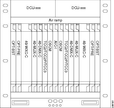
Figure 12-53 shows a functional block diagram of one line termination side using 40-WXC-C and 40-MUX-C cards.
Figure 12-53 Line Termination Mesh Node Side—40-MUX-C Cards
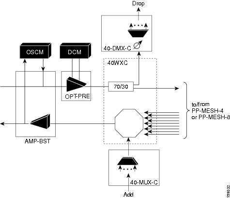
Figure 12-54 shows a functional block diagram line termination side using 40-WXC-C and 40-WSS-C cards.
Figure 12-54 Line Termination Mesh Node Side—40-WSS-C Cards
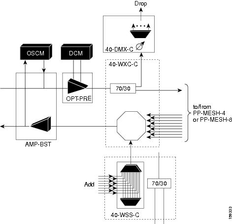
Figure 12-55 shows a functional block diagram of a node that interconnects a ROADM with MMU cards with two native line termination mesh sides.
Figure 12-55 Line Termination Mesh Nodes—ROADM With MMU Cards
12.7.1.1 40-Channel Omni-directional n-degree ROADM Node
Any side in the line termination mesh node can be configured as an omni-directional side. The side that is configured as the omni-directional side is connected to a local multiplexer and demultiplexer that can add or drop traffic to or from any of the node directions.
In Figure 12-56 side D is configured as the omni-directional side. Wavelengths from the local multiplexer on side D is routed to sides A, B, or C by the patch panel. Wavelengths from sides A, B, or C can be dropped on side D. The maximum number of omni-directional channels is 40.
Figure 12-56 40-Channel Omni-directional Four-Degree ROADM Node
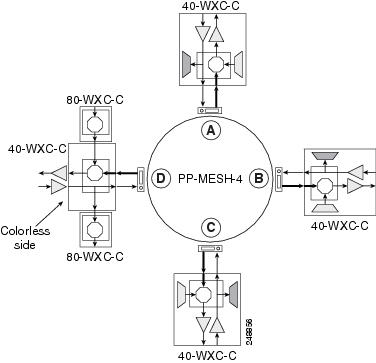
12.7.1.2 40-Channel Colorless n-Degree ROADM Node
Any side in the line termination mesh node can be configured as a colorless side where any wavelength can be added or dropped. The side that is configured as the colorless side is connected to two 80-WXC-C cards configured as a multiplexer and demultiplexer respectively. In Figure 12-57 side D is configured as the colorless side. The 80-WXC-C cards are connected to the add and drop ports of the 40-WXC-C cards and function as a colorless multiplexer and demultiplexer.
A combination of wavelengths from any of the nine ports is sent to the common output port of the 80-WXC-C card (multiplexer) that is connected to the 40-WXC-C card. The wavelengths entering the 40-WXC-C card are sent to the common input port of the 80-WXC-C card (demultiplexer) and dropped at any of the nine output ports.
Figure 12-57 40-Channel Colorless Four-Degree ROADM Node
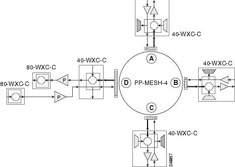
12.7.1.3 40-Channel Colorless and Omni-directional n-Degree ROADM Node
Any side in the line termination mesh node can be configured as a colorless and omni-directional side. The side that is configured as the colorless and omni-directional side is connected to a multiplexer (80-WXC-C) and demultiplexer (80-WXC-C) that can add or drop traffic to or from any of the node directions.
Figure 12-58 shows the layout of a 40-channel n-degree ROADM node with colorless and omni-directional side.
Figure 12-58 40-Channel n-Degree ROADM Node with Colorless and Omni-directional Side
In Figure 12-59 side D is configured as the colorless and omni-directional side.
A combination of wavelengths from any of the nine ports is sent to the common output port of the 80-WXC-C card (multiplexer) and then routed to the preamplifier. The preamplifier sends the wavelengths to the 40-WXC-C card that is connected to the patch panel. The patch panel routes the wavelengths to sides A, B, or C.
Wavelengths from sides A, B, or C are dropped on side D. The incoming wavelengths from the 40-WXC-C card are sent to the preamplifier. The preamplifier amplifies the signal and sends it to the common input port of the 80-WXC-C card (demultiplexer). The wavelengths are then dropped at any of the nine output ports.
Figure 12-59 40-Channel Colorless and Omni-directional Four-Degree ROADM Node
12.7.2 Line Termination Mesh Node Using 80-WXC-C Cards
Line termination mesh nodes using 80-WXC-C cards can support between one and eight line terminations. Each line direction requires the following units: 80-WXC-C, 15216-MD-40-ODD, 15216-EF-40-ODD, or 15216-MD-48-ODD, and 15216-MD-40-EVEN, 15216-EF-40-EVEN, or 15216-MD-48-EVEN, 15216-MD-ID-50 or 15216-MD-48-CM, a preamplifier, and a booster.
- The OPT-BST cards can be replaced with OPT-AMP-17-C (in OPT-BST mode) or OPT-BST-E cards.
- The OPT-PRE can be replaced with an OPT-AMP-17-C (in OPT-LINE mode) card.
Each side of the line termination mesh node is connected as follows:
- The 80-WXC-C COM-RX port is connected to the preamplifier output port.
- The 80-WXC-C COM port is connected to the booster amplifier COM-RX port.
- The 80-WXC-C DROP TX port is connected to the COM-RX (ODD+EVEN-RX) port of 15216-MD-ID-50 or 15216-MD-48-CM. The ODD-TX port of the 15216-MD-ID-50 or 15216-MD-48-CM is connected to the COM-RX port of 15216-MD-40-ODD, 15216-EF-40-ODD, or 15216-MD-48-ODD; and the EVEN-TX port of the 15216-MD-ID-50 or 15216-MD-48-CM is connected to the COM-RX port of 15216-MD-40-EVEN, 15216-EF-40-EVEN, or 15216-MD-48-EVEN.
- The 80-WXC-C AD port is connected to the COM-TX (ODD+EVEN-TX) port of 15216-MD-ID-50 or 15216-MD-48-CM. The ODD-RX port of the 15216-MD-ID-50 or 15216-MD-48-CM is connected to the COM-TX port of 15216-MD-40-ODD, 15216-EF-40-ODD, or 15216-MD-48-ODD; and the EVEN-RX port of the 15216-MD-ID-50 or 15216-MD-48-CM is connected to the COM-TX port of 15216-MD-40-EVEN, 15216-EF-40-EVEN, or 15216-MD-48-EVEN.
- The 80-WXC-C EXP-TX port is connected to the mesh patch panel.
Figure 12-60 shows the layout for a line termination node.
Figure 12-60 Line Termination Node
Figure 12-61 shows the functional block diagram of a four-degree line termination mesh node using 80-WXC-C, 15216-MD-40-ODD, 15216-EF-40-ODD, 15216-MD-48-ODD, 15216-MD-40-EVEN, 15216-EF-40-EVEN, or 15216-MD-48-EVEN and a PP MESH-4. Wavelengths entering from side(i) can be routed to any of the other n-1 sides where n is defined by the PP MESH type.
Figure 12-61 Four-Degree Line Termination Mesh Node Functional Diagram
12.7.2.1 80-Channel Omni-directional n-degree ROADM Node
Any side in the line termination mesh node can be configured as a omni-directional side. The side that is configured as the omni-directional side is connected to a local multiplexer and demultiplexer that can add or drop traffic to or from any of the node directions.
In Figure 12-62, side D is configured as the omni-directional side. Wavelengths from the local multiplexer on side D are routed to sides A, B, or C by the patch panel. Wavelengths from sides A, B, or C are dropped on side D.
Figure 12-62 80-Channel Omni-directional Four-Degree ROADM Node
12.7.2.2 80-Channel Colorless n-degree ROADM Node
Any side in the line termination mesh node can be configured as a colorless side where any wavelength can be added or dropped. The side that is configured as the colorless side is connected to two 80-WXC-C cards configured as a multiplexer and demultiplexer respectively. In Figure 12-63, side D is configured as the colorless side. The 80-WXC-C cards are connected to the add and drop ports of the 80-WXC-C cards as a colorless multiplexer and demultiplexer.
A combination of wavelengths from any of the nine ports is sent to the common output port of the 80-WXC-C card (multiplexer) that is connected to the 80-WXC-C card. The wavelengths entering the 80-WXC-C card is passed to the common input port of the 80-WXC-C card (demultiplexer) and dropped at any of the nine output ports.
Figure 12-63 80-Channel Colorless Four-Degree ROADM Node
12.7.2.3 80-Channel Colorless and Omni-directional n-Degree ROADM Node
Any side in the line termination mesh node can be configured as a colorless and omni-directional side. The side that is configured as the colorless and omni-directional side is connected to a multiplexer (80-WXC-C) and demultiplexer (80-WXC-C) that can add or drop traffic to or from any of the node directions.
Figure 12-64 shows the layout of a 80-channel n-degree ROADM node with colorless and omnidirectional side.
Figure 12-64 80-Channel n-degree ROADM Node with Colorless and Omnidirectional Side
In Figure 12-65 side D is configured as the colorless and omni-directional side.
A combination of wavelengths from any of the nine ports is sent to the common output port of the 80-WXC-C card (multiplexer) and is then routed to the preamplifier. The preamplifier sends the wavelengths to the 80-WXC-C card that is connected to the patch panel. The patch panel routes the wavelengths to sides A, B, or C.
Wavelengths from sides A, B, or C can be dropped on side D. The incoming wavelengths from the 80-WXC-C card are sent to the preamplifier. The preamplifier amplifies the signal and sends it to the common input port of the 80-WXC-C card (demultiplexer). The wavelengths are then dropped at any of the nine output ports.
Figure 12-65 80-Channel Colorless and Omni-directional Four-Degree ROADM Node
12.7.3 Line Termination Mesh Node Using 40-SMR2-C Cards
Line termination mesh nodes using the 40-SMR2-C cards can support between one and four line terminations. Each line direction requires the 40-SMR2-C and 15216-MD-40-ODD, 15216-EF-40-ODD, or 15216-MD-48-ODD units. Although it is recommended that you use the 15216-MD-40-ODD, 15216-EF-40-ODD, or 15216-MD-48-ODD patch panel along with the 40-SMR2-C card, you can alternatively use the 40-MUX-C and 40-DMX-C cards instead of the 15216-MD-40-ODD, 15216-EF-40-ODD, or 15216-MD-48-ODD patch panel.
Each side of the line termination mesh node is connected as follows:
- The 40-SMR2-C LINE-RX port is connected to the external line.
- The 40-SMR2-C LINE-TX port is connected to the external line.
- The 40-SMR2-C DROP TX port is connected to the 15216-MD-40-ODD, 15216-EF-40-ODD, or 15216-MD-48-ODD (or 40-DMX-C) COM-RX port.
- The 40-SMR2-C ADD-RX port is connected to the 15216-MD-40-ODD, 15216-EF-40-ODD, or 15216-MD-48-ODD (or 40-MUX-C) COM-TX port.
- The 40-SMR2-C EXP-TX port is connected to the mesh patch panel.
- The 40-SMR2-C EXP i -RX (where i = 1, 2, 3) port is connected to the mesh patch panel.
Figure 12-66 shows the layout for a line termination node.
Figure 12-66 Line Termination Mesh Node Shelf
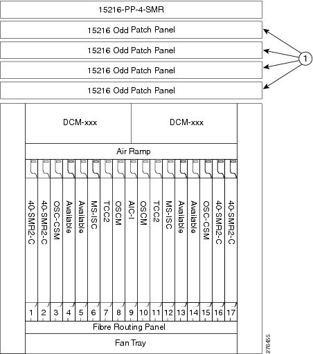
Figure 12-67 shows the functional block diagram of a four-degree line termination mesh node using 40-SMR2-C, 15216-MD-40-ODD, 15216-EF-40-ODD, or 15216-MD-48-ODD, and 15454-PP-4-SMR patch panel.
Figure 12-67 Four-Degree Line Termination Mesh Node Functional Diagram
12.7.4 XC Termination Mesh Node
The XC termination mesh node, shown in Figure 12-68, is the second mesh node type. It is used to upgrade a non-mesh node to a mesh node or to interconnect two non-mesh nodes. The XC termination mesh nodes contain the following cards:
The XC termination mesh node is connected as follows:
- The 40-WXC-C COM-RX port is connected to the MMU EXP-A-TX port.
- The 40-WXC-C COM-TX port is connected to the MMU EXP-A-RX port.
- The 40-WXC-C EXP-TX port is connected to the OPT-AMP-17-C COM-RX port.
- The 40-WXC-C EXP-RX port is connected to the OPT-AMP-17-C COM-TX port.
- The 40-WXC-C EXP-TX port is connected to the mesh patch panel.
- The 40-WXC-C EXP-RX port is connected to the mesh patch panel.
Figure 12-68 XC Termination Mesh Node Shelf
12.7.5 Mesh Patch Panels and Shelf Layouts
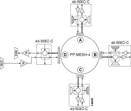
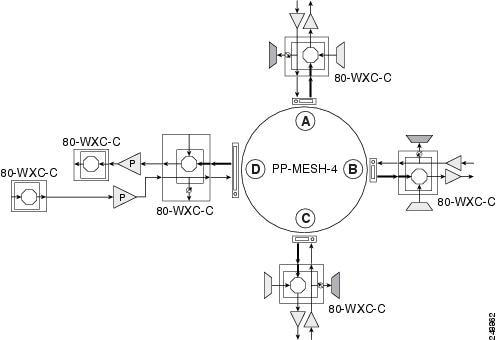
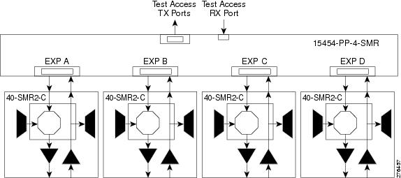
ONS 15454 mesh topologies require the installation of a four-degree patch panel, PP-MESH-4 (for 40-WXC-C cards) or 15454-PP-4-SMR (for 40-SMR2-C cards) or an eight-degree patch panel, PP-MESH-8 (for 40-WXC-C cards). If the four-degree patch panel is installed, mesh topologies of up to four degrees can be created. If the eight-degree patch panel is installed, mesh topologies of up to eight degrees can be created. The four-degree patch panel contains four 1x4 optical splitters, and the eight-degree patch panel contains eight 1x8 splitters. Each mesh patch panel contains a 2x8 splitter that is used for the test access transmit and receive ports. Figure 12-69 shows a block diagram for the PP-MESH-4 patch panel.
Figure 12-69 PP-MESH-4 Patch Panel Block Diagram
At the mesh patch panel, the signal is split into four signals (if a four-degree patch panel is used) or eight signals (if an eight-degree patch panel is used). Figure 12-70 shows the signal flow at the four-degree PP-MESH-4 patch panel. 40-WXC-C cards connect to the four-degree patch panel at the EXP TX and COM RX ports.
Figure 12-70 PP-MESH-4 Patch Panel Signal Flow
The mesh patch panels interconnect 40-WXC-C cards to create mesh networks, including four-degree and eight-degree mesh topologies. In addition, shelves with 40-WXC-C cards can be configured with mesh patch panels to create multiring, MMU-based mesh nodes. 40-WXC-C cards can be installed in ROADM nodes with MMU cards to upgrade a two-degree MMU-based ROADM node into four-degree or eight-degree mesh nodes.
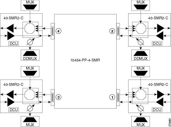
Figure 12-71 shows the block diagram of the four-degree 15454-PP-4-SMR patch panel connected to one 40-SMR2-C card. The 40-SMR2-C cards connect to the 15454-PP-4-SMR patch panel at the EXP RX ports.
Figure 12-71 15454-PP-4-SMR Patch Panel Block Diagram
You can use the 15454-PP-4-SMR patch panel to connect up to four 40-SMR2-C cards in a four-degree mesh node. The optical splitters inside the patch panel forward the output signal (EXP-TX port) of the 40-SMR2-C card on each side of the mesh node to the input port of the 40-SMR2-C cards on the other three sides of the mesh node. The 4x1 WXC block inside the 40-SMR2-C card selects which wavelength from which side must be propagated at the output of each side. Figure 12-70 shows the signal flow at the four-degree 15454-PP-4-SMR patch panel. 40-SMR2-C cards connect to the four-degree patch panel at the EXP-TX and EXP-RX ports.
Figure 12-72 15454-PP-4-SMR Patch Panel Signal Flow
12.7.6 Using a Mesh Node With Omni-Directional Add/Drop Section
Normally, multidegree mesh node use four or eight 40-WXC-C cards and a four-degree or eight-degree patch panel. Each of the 40-WXC-C cards uses a 40-MUX-C card to add wavelengths going to the span and a 40-DMX-C card to drop wavelengths coming in from the span. The 40-MUX-C and 40-DMX-C cards are connected to only one of the node directions. These cards can add/drop traffic only to/from the side that is associated to the 40-WXC-C card. The omni-directional configuration allows you to install a local multiplexer/demultiplexer that can add/drop traffic to/from any of the node directions. Figure 12-73 shows an example of how to set up a omni-directional add/drop configuration.
By setting up a NE as shown in the figure, it is possible to connect the transmit ports of TXP or MXP cards to a 40-MUX-C card and then connect the output of the 40-MUX-C card to an OPT-BST card. The OPT-BST card then connects to a preferred 40-WXC-C card in the four-degree or eight-degree ROADM node (40-WXC-C connected to port 4 of PP-MESH-4, as shown in the figure).
The patch panel splits the traffic coming from the OPT-BST card in all the node directions, through the software configuration. The wavelengths entering the 40-WXC-C cards (ports 1, 2, and 3) can be selectively sent out in any desired outbound direction. In the inbound direction, the patch panel on the preferred 40-WXC-C card, splits any of the wavelengths entering the NE through the 40-WXC-C cards (ports 1, 2, and 3). Through the software configuration, the wavelength can be passed to an OPT-PRE card or stopped. This whole configuration can be managed using a single IP address
An example of using a mesh node for omni-directional add/drop section is shown in Figure 12-73.
Figure 12-73 Mesh Node With Omni-Directional Add/Drop Section
12.8 DWDM Node Cabling
DWDM node cabling is specified by the Cisco TransportPlanner Internal Connections table. The following sections provide examples of the cabling that you will typically install for common DWDM node types.
Note The cabling illustrations shown in the following sections are examples. Always install fiber-optic cables based on the Cisco TransportPlanner Internal Connections table for your site.
12.8.1 OSC Link Termination Fiber-Optic Cabling
OSC link termination cabling include the following characteristics:
- The OPT-BST and OSC-CSM cards are the only cards that directly interface with the line (span) fiber.
- The OSCM card only carries optical service channels, not DWDM channels.
- The OSCM and OSC-CSM cards cannot both be installed on the same side of the shelf (Side B or Side A). You can have different cards on each side, for example an OSCM card on Side A and an OSC-CSM card on Side B.
- When an OPT-BST card and an OSC-CSM card are both used on the same side of the node, the OPT-BST card combines the supervision channel with the DWDM channels and the OSC-CSM card acts as an OSCM card; it does not carry DWDM traffic.
- If an OPT-BST and an OSCM card are installed on Side B, the Side B OPT-BST OSC RX port is connected to the Side B OSCM TX port, and the Side B OPT-BST OSC TX port is connected to the Side B OSCM RX port.
- If an OPT-BST and an OSC-CSM card are installed on Side B, the Side B OPT-BST OSC RX port is connected to the Side B OSC-CSM LINE TX port, and the Side B OPT-BST OSC TX port is connected to the Side B OSC-CSM LINE RX port.
- If an OPT-BST and an OSCM card are installed on Side A, the Side A OPT-BST OSC TX port is connected to the Side A OSCM RX port, and the Side A OPT-BST OSC RX port is connected to the Side A OSCM TX port.
- If an OPT-BST and an OSC-CSM card are installed on Side A, the Side A OPT-BST OSC TX port is connected to the Side A OSC-CSM LINE RX port, and the Side A OPT-BST OSC RX port is connected to the Side A OSC-CSM LINE TX port.
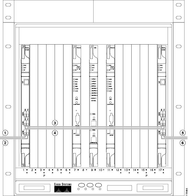
Figure 12-74 shows an example of OSC fibering for a hub node with OSCM cards installed.
Figure 12-74 Fibering OSC Terminations—Hub Node with OSCM Cards
12.8.2 Hub Node Fiber-Optic Cabling
The following rules generally apply to hub node cabling:
- The Side A OPT-BST or OSC-CSM card common (COM) TX port is connected to the Side A OPT-PRE COM RX port or the Side A 32DMX-O/40-DMX-C/40-DMX-CE COM RX port.
- The Side A OPT-PRE COM TX port is connected to the Side A 32DMX-O/40-DMX-C/40-DMX-CE COM RX port.
- The Side A 32MUX-O/32WSS/32WSS-L COM TX port is connected to the Side A OPT-BST or Side A OSC-CSM COM RX port.
- The Side B 32MUX-O/32WSS/32WSS-L COM TX port is connected to the Side B OPT-BST or Side B OSC-CSM COM RX port.
- The Side B OPT-BST or Side B OSC-CSM COM TX port is connected to the Side B OPT-PRE COM RX port or the Side B 32DMX-O/32DMX COM RX port.
- The Side B OPT-PRE COM TX port is connected to the Side B 32DMX-O/32DMX COM RX port.
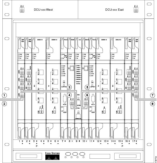
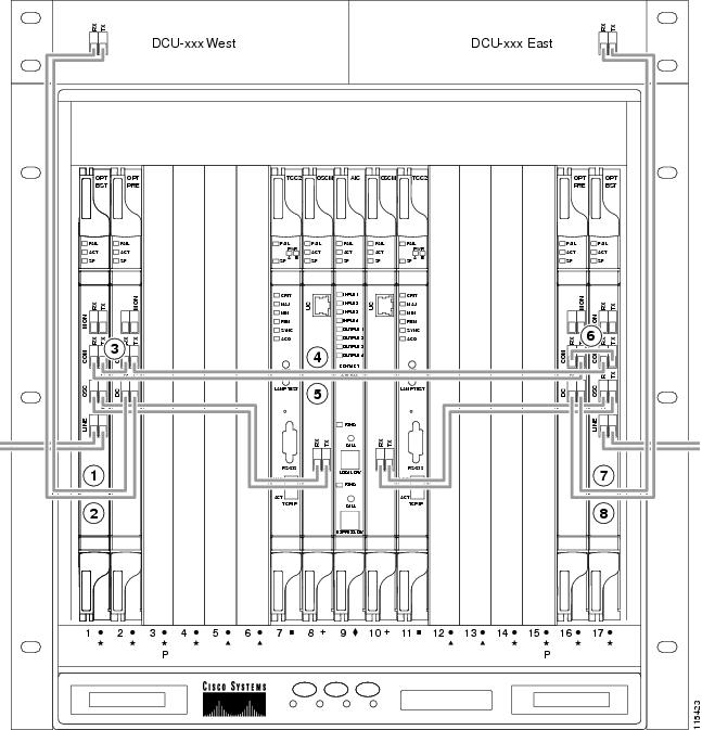
Figure 12-75 shows an example of a hub node with cabling. In the example, OSCM cards are installed. If OSC-CSM cards are installed, they are usually installed in Slots 1 and 17.
Figure 12-75 Fibering a Hub Node
Side A DCU TX to Side A OPT-PRE DC RX3 |
|||
12.8.3 Terminal Node Fiber-Optic Cabling
The following rules generally apply to terminal node cabling:
- A terminal site has only one side (as compared to a hub node, which has two sides). The terminal side can be either Side B or Side A.
- The terminal side OPT-BST or OSC-CSM card COM TX port is connected to the terminal side OPT-PRE COM RX port or the 32DMX-O/40-DMX-C/40-DMX-CE COM RX port.
- The terminal side OPT-PRE COM TX port is connected to the terminal side 32DMX-O/40-DMX-C/40-DMX-CE COM RX port.
- The terminal side 32MUX-O/40-MUX-C COM TX port is connected to the terminal side OPT-BST or OSC-CSM COM RX port.
12.8.4 Line Amplifier Node Fiber-Optic Cabling
The following rules generally apply to line amplifier node cabling:
- The line amplifier node layout allows all combinations of OPT-PRE and OPT-BST cards and allows you to use asymmetrical card choices in Side A-to-Side B and Side B-to-Side A configurations. For a given line direction, you can configure the four following possibilities:
– Only preamplification (OPT-PRE)
– Only booster amplification (OPT-BST)
– Both preamplification and booster amplification (where a line amplifier node has amplification in at least one direction)
– Neither preamplification nor booster amplification
– The Side A OSC-CSM or OPT-BST COM TX is connected to the Side A OPT-PRE COM RX port.
– The Side A OPT-PRE COM TX port is connected to the Side B OSC-CSM or OPT-BST COM RX port.
– The Side B OSC-CSM or OPT-BST COM TX port is connected to the Side B OPT-PRE COM RX port.
– The Side B OPT-PRE COM TX port is connected to the Side A OSC-CSM or OPT-BST COM RX port.
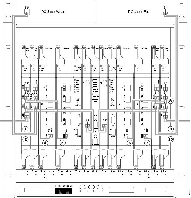
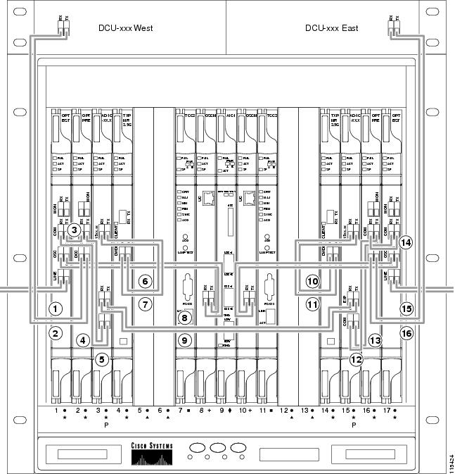
Figure 12-76 shows an example of a line amplifier node with cabling.
Figure 12-76 Fibering a Line Amplifier Node
Side A DCU TX to Side A OPT-PRE DC RX4 |
|||
12.8.5 OSC Regeneration Node Fiber-Optic Cabling
The following rules generally apply to OSC regeneration node cabling:
Figure 12-77 shows an example of an OSC regeneration node with cabling.
Figure 12-77 Fibering an OSC Regeneration Node
12.8.6 Amplified or Passive OADM Node Fiber-Optic Cabling
The two sides of the OADM node do not need to be symmetrical. On each side, Cisco TransportPlanner can create one of the following four configurations:
Note Amplified OADM nodes contain OPT-PRE cards and/or OPT-BST cards. Passive OADM nodes do not. Both contain add/drop channel or band cards.
The following rules generally apply for OADM node express path cabled connections:
- TX ports should only be connected to RX ports.
- EXP ports are connected only to COM ports in between AD-xC-xx.x or AD-xB-xx.x cards that all belong to Side B (that is, they are daisy-chained).
- EXP ports are connected only to COM ports in between AD-xC-xx.x or AD-xB-xx.x cards that all belong to Side A (that is, they are daisy-chained).
- The EXP port of the last AD-xC-xx.x or AD-xB-xx.x card on Side A is connected to the EXP port of the first AD-xC-xx.x or AD-xB-xx.x card on Side B.
- The OPT-BST COM RX port is connected to the nearest (in slot position) AD-xC-xx.x or AD-xB-xx.x COM TX port.
- The OPT-PRE COM TX port is connected to the nearest (in slot position) AD-xC-xx.x or AD-xB-xx.x COM RX port.
- If OADM cards are located in adjacent slots, the TCC2/TCC2P/TCC3/TNC/TNCE/TSC/TSCE card assumes that they are connected in a daisy-chain between the EXP ports and COM ports as noted previously.
- The first Side A AD-xC-xx.x or AD-xB-xx.x card COM RX port is connected to the Side A OPT-PRE or OSC-CSM COM TX port.
- The first Side A AD-xC-xx.x or AD-xB-xx.x card COM TX port is connected to the Side A OPT-BST or OSC-CSM COM RX port.
- The first Side B AD-xC-xx.x or AD-xB-xx.x card COM RX port is connected to the Side B OPT-PRE or OSC-CSM COM TX port.
- The first Side B AD-xC-xx.x or AD-xB-xx.x card COM TX port is connected to the Side B OPT-BST or OSC-CSM RX port.
- If a Side A OPT-PRE is present, the Side A OPT-BST or OSC-CSM COM TX port is connected to the Side A OPT-PRE COM RX port.
- If a Side B OPT-PRE is present, the Side B OPT-BST or OSC-CSM COM TX port is connected to the Side B OPT-PRE COM RX port.
The following rules generally apply for OADM node add/drop path cabled connections:
– 4MD-xx.x COM TX or 4MD-xx.x COM RX ports
– Another AD-xB-xx.x add/drop port (a pass-through configuration)
- An AD-xB-xx.x add/drop band port is only connected to a 4MD-xx.x card belonging to the same band.
- For each specific AD-xB-xx.x card, the add and drop ports for that band card are connected to the COM TX and COM RX ports of the same 4MD-xx.x card.
- The AD-xB-xx.x and 4MD-xx.x cards are located in the same side (the connected ports all have the same line direction).
The following rules generally apply for OADM node pass-through path cabled connections:
- Pass-through connections are only established between add and drop ports on the same band or channel and in the same line direction.
- AD-xC-xx.x or AD-xB-xx.x add/drop ports must be connected to other AD-xC-xx.x or AD-xB-xx.x add/drop ports (as pass-through configurations).
- Add (RX) ports must be connected to drop (TX) ports.
- 4MD-xx.x client input/output ports must be connected to other 4MD-xx.x client input/output ports.
- A Side A AD-xB-xx.x drop (TX) port is connected to the corresponding Side A 4MD-xx.x COM RX port.
- A Side A AD-xB-xx.x add (RX) port is connected to the corresponding Side A 4MD-xx.x COM TX port.
- An Side B AD-xB-xx.x drop (TX) port is connected to the corresponding Side B 4MD-xx.x COM RX port.
- An Side B AD-xB-xx.x add (RX) port is connected to the corresponding Side B 4MD-xx.x COM TX port.
Figure 12-78 shows an example of an amplified OADM node with AD-1C-xx.x cards installed.
Note Figure 12-78 is an example. Always install fiber-optic cables based on the Cisco TransportPlanner Internal Connections table for your site.
Figure 12-78 Fibering an Amplified OADM Node
Side A DCU TX to Side A OPT-PRE DC RX5 |
|||
Side B TXP_MR_2.5G DWDM RX to Side B AD-1C-xx.x (15xx.xx) TX |
|||
Side B TXP_MR_2.5G DWDM TX to Side B AD-1C-xx.x (15xx.xx) RX |
|||
Side A AD-1C-xx.x (15xx.xx) RX to Side A TXP_MR_2.5G DWDM TX |
|||
Side A AD-1C-xx.x (15xx.xx) TX to Side A TXP_MR_2.5G DWDM RX |
|||
Figure 12-79 shows an example of a passive OADM node with two AD-1C-xx.x cards installed.
Figure 12-79 Fibering a Passive OADM Node
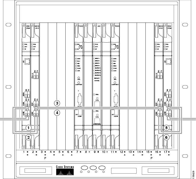
12.8.7 ROADM Node Fiber-Optic Cabling
The following rules generally apply to ROADM node cabling:
- The Side A OPT-BST or OSC-CSM COM TX port is connected to the Side A OPT-PRE COM RX port.
- The Side A OPT-PRE COM TX port is connected to the Side A 32WSS COM RX port.
- The Side A OPT-BST or OSC-CSM COM RX port is connected to the Side A 32WSS COM TX port.
- The Side A OPT-BST (if installed) OSC TX port is connected to the Side A OSCM RX port.
- The Side A OPT-BST (if installed) OSC RX port is connected to the Side A OSCM TX port.
- The Side A 32WSS EXP TX port is connected to the Side B 32WSS EXP RX port.
- The Side A 32WSS EXP RX port is connected to the Side B 32WSS EXP TX port.
- The Side A 32WSS DROP TX port is connected to the Side A 32DMX COM RX port.
- The Side A 40-WSS-C/40-WSS-CE DROP TX port is connected to the Side A 40-DMX-C or 40-DMX-CE COM RX port.
- The Side B OPT-BST or OSC-CSM COM TX port is connected to the Side B OPT-PRE COM RX port.
- The Side B OPT-PRE COM TX port is connected to the Side B 32WSS COM RX port.
- The Side B OPT-BST or OSC-CSM COM RX port is connected to the Side B 32WSS COM TX port.
- The Side B OPT-BST (if installed) OSC TX port is connected to the Side B OSCM RX port.
- The Side B OPT-BST (if installed) OSC RX port is connected to the Side B OSCM TX port.
- The Side B 32WSS DROP TX port is connected to the Side B 32DMX COM RX port.
- The Side B 40-WSS-C/40-WSS-CE DROP TX port is connected to the Side B 40-DMX-C or 40-DMX-CE COM RX port.
Figure 12-80 shows an example of an amplified ROADM node with cabling.
Note Figure 12-80 is an example. Always install fiber-optic cables based on the Cisco TransportPlanner Internal Connections table for your site.
Figure 12-80 Fibering a ROADM Node
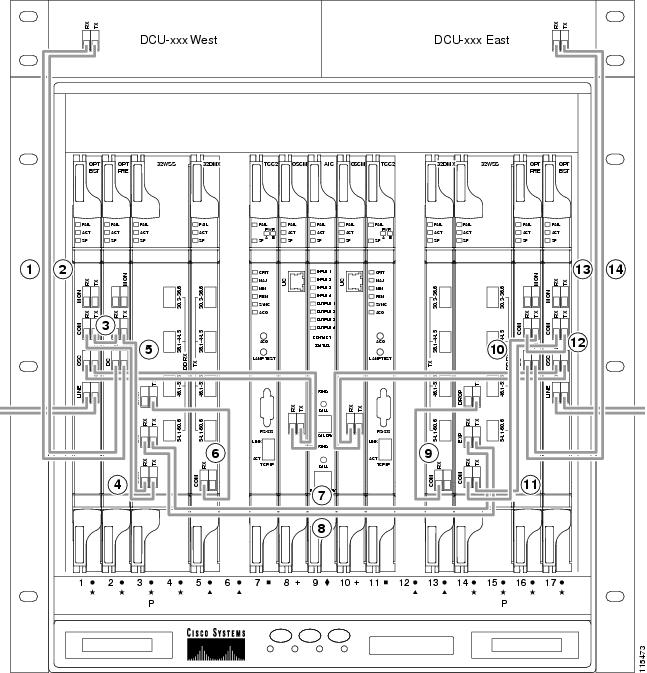
Side A DCU TX to Side A OPT-PRE DC RX6 |
|||
12.9 Automatic Node Setup
Automatic node setup (ANS) is a TCC2/TCC2P/TCC3/TNC/TNCE/TSC/TSCE function that adjusts values of the variable optical attenuators (VOAs) on the DWDM channel paths to equalize the per channel power at the amplifier input. This power equalization means that at launch, all channels have the same amplifier power, independent of the input signal on the client interface and independent of the path crossed by the signal inside the node. This equalization is needed for two reasons:
- Every path introduces a different penalty on the signal that crosses it.
- Client interfaces add their signal to the ONS 15454 DWDM ring with different power levels.
To support ANS, integrated VOAs and photodiodes are provided in the following cards:
- AD-xB-xx.x card express and drop paths
- AD-xC-xx.x card express and add paths
- 4MD-xx.x card add paths
- 32MUX-O card add paths
- 32WSS/40-WSS-C/40-WSS-CE/40-WXC-C/80-WXC-C add, drop, and pass through paths
- 32DMX-O card drop paths
- 32DMX, 40-DMX-C, 40-DMX-CE card input port
- 40-MUX-C card output port
- 40-SMR1-C/40-SMR2-C add, drop, and pass through ports
- PSM card input and output ports (both working and protect path)
Optical power is equalized by regulating the VOAs. Based on the expected per channel power, ANS automatically calculates the VOA values by:
- Reconstructing the different channel paths.
- Retrieving the path insertion loss (stored in each DWDM transmission element).
VOAs operate in one of three working modes:
- Automatic VOA Shutdown—In this mode, the VOA is set at maximum attenuation value. Automatic VOA shutdown mode is set when the channel is not provisioned to ensure system reliability in the event that power is accidentally inserted.
- Constant Attenuation Value—In this mode, the VOA is regulated to a constant attenuation independent from the value of the input signal. Constant attenuation value mode is set on VOAs associated to aggregated paths.
- Constant Power Value—In this mode, the VOA values are automatically regulated to keep a constant output power when changes occur to the input power signal. This working condition is set on VOAs associated to a single channel path.
ANS calculates the following VOA provisioning parameters:
Optical patchcords are passive devices that are modeled by the two termination points, each with an assigned slot and port. If user-provisioned optical patchcords exist, ANS checks if the new connection is feasible according to internal connection rules. If the user connection violates one of the rules, ANS returns a denied message. ANS requires the expected wavelength to be provisioned. When provisioning the expected wavelength, the following rules apply:
- The card family generically characterizes the card name, and not the particular wavelengths supported (for example, AD-2C-xx.x for all two-channel OADMs).
- At the provisioning layer, you can provision a generic card for a specific slot using CTC or TL1.
- Wavelength assignment is done at the port level.
- An equipment mismatch alarm is raised when a mismatch between the identified and provisioned value occurs. The default value for the provisioned attribute is AUTO.
ONS 15454 ANS parameters set the values required for the node to operate successfully. Cisco Transport Planner calculates the ANS parameters based on the requirements of a planned network. Cisco Transport Planner exports the parameters to NE update file. When the NE update file is imported in CTC, the Provisioning > WDM-ANS > Provisioning tab is populated with the ANS parameters to provision the node for the network. These ANS parameters can be modified even when the card port is in IS state. All the ANS parameters are mapped to the physical ports of the cards. ANS parameters can also be manually added, modified, or deleted in the Provisioning tab. ANS parameters cannot be deleted when the port is in IS state and if any active circuit uses the ANS parameters. If the new or updated value is not within the default range as shown in Table 12-11, an error message is displayed. For more information on how to add, modify, or delete an ANS parameter, see the G328 Add, Modify, or Delete ANS Parameters.
Note The Provisioning > WDM-ANS > Provisioning tab in CTC is empty if the NE update file is not imported.
Note It is recommended that you use the Cisco Transport Planner NE Update file to provision the ANS parameters instead of manually adding all the parameters in CTC. ANS provisioning parameters must be manually changed by Cisco qualified personnel only. Setting incorrect ANS provisioning (either as preamplifier or booster input power thresholds) may impact traffic.
Yes7 |
||
Raman Expected Gain8 |
||
Yes9 |
||
Yes10 |
||
|
7.Per-channel power and tilt can be edited when the Amplifier Working Mode is Control Gain or Control Power and Fixed Gain when Amplifier Working Mode is Fixed Gain |
ANS parameters can be viewed in the node view Provisioning > WDM-ANS > Provisioning tab, as shown in Figure 12-81.
Figure 12-81 WDM-ANS Provisioning
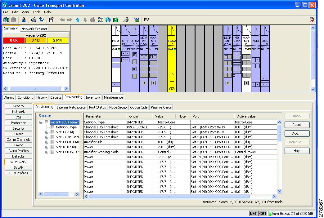
The Provisioning > WDM-ANS > Provisioning tab presents the following information:
- Selector—Presents the ANS parameters in a tree view based on physical position. Clicking the + or – expands or collapses individual tree elements. Clicking a tree element displays the element parameters in the table on the right. For example, clicking the node name at the top displays all the node ANS parameters or clicking Slot 1 (PSM) displays the PSM amplifier parameters only. The ANS parameters can be sorted according to physical position.
- Parameter—Displays the ANS parameter name.
- Origin—Indicates how the parameter was calculated:
– Imported—The value was set by importing the CTP XML file.
– Provisioned—The value was manually provisioned.
– Automatic—The value is automatically calculated by the system using the Raman provisioning wizard. For more information on how to provision using a wizard, see the G468 Configure the Raman Pump Using the Installation Wizard.
- Value—Displays the ANS parameter value. The values can be modified manually, although manually modifying the ANS parameters is not recommended.
- Note—Displays information for parameters that could not be calculated, that is, parameters with Unknown appearing in the Value column.
- Port —Displays the port value. Port is represented as Slot.Port.
- Active Value —Displays the active parameter value. The active value cannot be modified manually. When you modify the parameter value in the Value field, the active value is updated with the modified value after you run ANS.
The Provisioning > WDM-ANS > Port Status tab presents the following information:
- Port—Displays the port value. The port is represented as Slot.Port.
- Parameter—Displays the ANS parameter name.
- Result—After you run ANS, the status for each ANS parameter in the Results column is provided:
– Success - Changed—The parameter setpoint was recalculated successfully.
– Fail - Out of Range—The calculated setpoint is outside the expected range.
– Fail - Missing Input Parameter—The parameter could not be calculated because the required provisioning data is unknown or unavailable.
– Not Applicable State—Ports are not in use.
- Value—Displays the parameter value.
- Set By—Displays the application that sets this parameter. This field can take the following values:
A parameter could be set by more than one application. For example, VOA Attenuation parameter could be set by both ANS and APC. In this case, individual entries will be displayed for ANS and APC.
12.9.1 ANS Parameters in a Raman Node With Post-Amplifiers
The following ANS parameters drive the node regulations in the Raman node:
- Power (DC-TX port)—It is the per channel output power level that is allowed on the embedded erbium-doped fiber amplifier (EDFA) amplification stage of the OPT-RAMP-C or OPT-RAMP-CE card. The power can be measured accurately only when the value of the internal VOA is set to 0 dB. During circuit creation, the Power (DC-TX port) setpoint is used to calculate the Gain of the embedded EDFA(G EDFA ) in the OPT-RAMP-C or OPT-RAMP-CE card. The G EDFA setpoint has a direct impact on the actual gain tilt that the embedded EDFA generates. If the value of the G EDFA is greater than or less than the optimum Gain (G OPTIMUM ) setpoint of the OPT-RAMP-C or OPT-RAMP-CE card, the output spectrum is affected by a positive or negative gain tilt.
The G OPTIMUM setpoints for the OPT-RAMP-C or OPT-RAMP-CE cards are:
The APC automatically calculates the gain tilt. The difference between the G OPTIMUM and G EDFA values of every 1 dB causes a gain tilt of 0.7 dB. Setting an appropriate counter-tilt setpoint on the first amplifier card that is present downstream of the embedded EDFA, compensates the gain tilt.
- Power (COM-TX port)—It is the per channel power level that is allowed on the COM-TX port of the OPT-RAMP-C or OPT-RAMP-CE card. The Power (COM-TX port) setpoint and the DCU insertion loss is used to calculate the attenuation value of the internal VOA of the OPT-RAMP-C or OPT-RAMP-CE card when the first circuit is provisioned. The Power (COM-TX port) setpoint ensures that the power levels at the input port of the amplifier cards (configured in the OPT-PRE or the OPT-LINE mode) downstream are stable. CTP generates the setpoint to suit the optimum Gain range of the amplifier card used.
- Power (LINE-TX port)—It is the per channel power setpoint that is allowed on the LINE-TX output port. The amplifiers that are present downstream of the OPT-RAMP-C card can be configured as OPT-PRE in ROADM nodes or as OPT-LINE in optical line amplifier (OLA) nodes. When the first circuit is provisioned, the Power (LINE-TX port) setpoint is used to automatically calculate the Gain.
- Amplifier Tilt (LINE-TX port)—It is the gain tilt (TILT CTP ) that CTP calculates based on the output power of the amplifier configured as OPT-PRE in ROADM nodes or as OPT-LINE in OLA nodes. This is the target value to be reached after circuit creation. The APC dynamically adjusts the tilt reference (TILT REFERENCE ) value to meet the target taking into consideration the Raman tilt (TILT RAMAN ) that the Raman installation wizard calculates and the EDFA tilt (TILT EDFA ) that is calculated by the OPT-RAMP-C or OPT-RAMP-CE card based on its G EDFA value:
12.9.2 ANS Parameters in a Raman Node Without Post-Amplifiers
The TCC automatically identifies the node layout as “Raman Only” and regulates the amplifiers and VOA.
The following ANS parameters drive the node regulations in the Raman node without post-amplifiers:
- Amplifier Tilt (DC-TX port)—CTP configures a predefined tilt value in the range of +/- 1.5 dB on the embedded EDFA, based on the optical characteristics of the fiber downstream of the OPT-RAMP-C or OPT-RAMP-CE card. The embedded EDFA amplifier in OPT-RAMP-C or OPT-RAMP-CE cards work in the fixed gain mode. The G EDFA is equal to the G OPTIMUM setpoint by default and ensures a flat output spectrum.
The G OPTIMUM setpoints of the OPT-RAMP-C or OPT-RAMP-CE cards are:
If the tilt reference value is not equal to zero, it has a direct impact on the G EDFA . The APC changes the tilt reference value and consequently the G EDFA by taking the system tilt contribution accumulated along the transmission line.
- POWER (LINE-TX port)—It is the maximum per channel power level that is allowed on the LINE-TX port of the OPT-RAMP-C, OPT-RAMP-CE, or OSC-CSM card in accordance to the node layout. CTP calculates this setpoint to ensure that the system does not suffer from non-linear effects. The APC can change the power levels based on the traffic pattern and fiber type but never exceeds the setpoint value.
12.9.3 Raman Setup and Tuning
Raman amplification occurs in the optical fiber and the consequent Raman gain depends on the characteristics of the span (attenuator presence, fiber type, junctions, etc.). As two Raman pumps at two different wavelengths are used to stimulate the Raman effect, not only is the total signal power calculation significant, but the right mix of power to ensure gain flatness is crucial. These set points of the total Raman power and Raman ratio can be configured on the OPT-RAMP-C or OPT-RAMP-CE card in three ways:
Raman amplification on OPT-RAMP-C or OPT-RAMP-CE cards depends on the optical fiber installed. Therefore, Raman total power and Raman ratio values calculated using the Raman installation wizard via CTC is more accurate than the values provisioned by loading the CTP XML file. For this reason, the value provisioned using the wizard cannot be overridden by the CTP XML file. However, the values provisioned using the wizard or the CTP XML file can be overriden by manually provisioning the parameters.
When the Raman installation is completed, a report of the status of Raman configuration on a node in the OPT-RAMP-C or OPT-RAMP-CE card can be viewed in the Maintenance > Installation tab when you are in card view.
The Installation tab displays the following fields:
- User—Name of user who configured the Raman pump.
- Date—Date when the Raman pump was configured.
- Status
– Raman Not Tuned—The OPT-RAMP-C or OPT-RAMP-CE card was provisioned but ANS was not launched.
– Tuned by ANS—ANS was run successfully and the basic ANS parameters were applied.
– Tuned by Wizard—The Raman installation wizard was run successfully without errors.
– Tuned by User Acceptance—The Raman installation wizard was completed with errors and the user accepted the values that the wizard calculated.
– Raman is Tuning—The Raman installation wizard is running.
- S1Low (dBm)—See Table 12-12 .
- S1High (dBm)—See Table 12-12 .
- S2Low (dBm)—See Table 12-12 .
- S2High (dBm)—See Table 12-12 .
- Power (mW)—Total Raman power set points.
- Ratio—Raman pump ratio setpoint.
- Gain—Expected Raman gain that the wizard calculated.
- Actual Tilt—Expected Raman tilt that the wizard calculated.
- Fiber Cut Recovery—Status of the fiber cut restoration.
– Executed—The restore procedure was completed successfully.
– Pending—The restore procedure is not complete.
– Failed—The system failed to execute the procedure.
The Raman pump is equipped with two different Raman pumps transmitting powers (P1 and P2) at two different wavelengths  1 and
1 and  2. During installation, the two pumps alternatively turn ON and OFF at two different power values.
  1 and
1 and  2 signals are used as probes at the end of spans to measure Raman gain efficiency of the two Raman pumps separately.
The example in Raman Gain on Node B shows the Raman gain on an OPT-RAMP-C or OPT-RAMP-CE card in Node B that was measured by setting the wavelength and power measurements as follows:
 1=1530.33 nm signal probe at Node A
 2=1560.61 nm signal probe at Node A
Figure 12-82 Raman Gain on Node B
The S1low, S1high, S2low, and S2low values in the Maintenance > Installation tab are based on the power values read on the LINE-RX port of Node B.
 1=1530.33 nm at Node A
 2=1560.61 nm at Node A
12.9.4 RAMAN-CTP and RAMAN-COP Card Start Up and Fiber Link Turn Up
The local and remote nodes, equipped with RAMAN-CTP and RAMAN-COP cards, must follow this sequence to startup the card and complete the Raman link turn up.
1. The distributed feedback laser must be enabled—The RAMAN-CTP cards are equipped with embedded distributed feedback (DFB) lasers that operate at 1568.77 nm. The DFB RX port is capable of detecting very low power levels (-55 dBm or -60 dBm). By default, the DFB laser is disabled and the DFB ports are in IS-AINS (ANSI)/Unlocked,automaticInService (ETSI) state. The DFB ports are moved to IS (ANSI)/Unlocked (ETSI) state and the laser is enabled in pulse mode, by performing either one of the following:
a. In a DCN Extension layout, ANS is launched. A side-to-side OTS provisionable patchcord (PPC) is created on the side of the node where the RAMAN-CTP card is installed after the DFB ports are successfully regulated (ports are in service). During the creation of the PPC, the TNC card moves the following ports to the IS (ANSI)/Unlocked (ETSI) state:
– Ports included in the optical path—LINE ports of the RAMAN-CTP card
– RAMAN-TX and ASE-RX ports of the RAMAN-CTP card
– RAMAN-TX port of the RAMAN-COP card (if the card is installed)
Note At this stage, the RAMAN ports do not emit power pulses even though they are in IS (ANSI)/Unlocked (ETSI) state.
b. In an OSC based layout, ANS is launched. An OSC termination is created on the side of the node where the RAMAN-CTP card is installed after the DFB ports are successfully regulated. During creation of the OSC termination, the TNC card moves the following ports to the IS (ANSI)/Unlocked (ETSI) state:
– Ports included in the optical path—LINE and COM ports of the RAMAN-CTP card and the LINE ports of the line amplifier
– RAMAN-TX and ASE-RX ports of the RAMAN-CTP card
– RAMAN-TX port of the RAMAN-COP card (if the card is installed)
Note At this stage, the RAMAN ports do not emit power pulses even though they are in IS (ANSI)/Unlocked (ETSI) state.
The DFB laser from the local node emits a 5-second pulse every 100 seconds and waits for a similar 5-second pulse in response from the DFB laser on the remote node.
Note For short spans, the DFB optical power level must be regulated by the internal VOA (working in constant power mode) using the provisioned value of the DFB power setpoint. The DFB power setpoint is limited to a maximum of +3 dBm.
2. The DFB laser link continuity is checked—The acknowledgement mechanism between the peer DFB modules works in the following manner:
– The DFB laser on the local node emits a 5-second pulse.
– The remote node detects a valid signal (value above the DFB LOS Optical Threshold) on the DFB-RX port and responds with a 9-second DFB laser pulse.
– The local node detects a signal from the remote DFB laser on the DFB-RX port and starts a counter to check the duration of the remote pulse.
– If the signal is detected for at least 9 seconds, link continuity is verified and the local node moves the DFB laser to steady (active) state.
– The remote node performs a similar signal validation and eventually the DFB link is active.
Note If the DFB-RX port detects a drop in the power below the threshold value before 9 seconds have elapsed, the procedure to check DFB link continuity is restarted.
Note If one of the fibers is down, the DFB signal must be in OFF state in the opposite fiber too. The acknowledgement mechanism automatically performs this action.
3. A check for short spans is performed—When the DFB signal is active, a point-to-point measurement of the span loss is done. The node measures the loss on the incoming span because the DFB signal is co-propagating. The insertion loss is the difference between the power value on the DFB-TX port of the remote node and the power value on the DFB-RX port of the local node. If the span loss is less than 20 dB, the RAMAN-CTP card raises the PWR-PROT-ON alarm on the RAMAN-TX port and the Raman pumps stop the startup procedure.
4. Excessive back reflection on RAMAN-CTP cards is checked—After the span loss check is complete, the Raman pumps on the RAMAN-CTP card on the local node are turned on in Automatic Power Reduction (APR) mode at reduced power (10 mW) lasting for 200 ms. The RAMAN-CTP cards perform a back reflection power test using an embedded fail threshold, which is configured during card production. The back reflection test lasts for 500 ms at the maximum. If the back reflection test is successful, the sequence continues with Step 5. If the check fails, the RAMAN-CTP get stuck with the DFB laser in ON state and the Raman pumps do not switch to full power. A Raman Laser Shutdown (RLS) alarm is raised on the RAMAN-TX port, where the failure is detected.
5. Excessive back reflection on RAMAN-COP cards is checked, if the RAMAN-COP cards are installed—The Raman pumps on the RAMAN-CTP card on the local node must shut down after the back reflection test is successful. This allows the same check to be executed by the RAMAN-COP card on the local node without any interference from the RAMAN-CTP card remnant signal.
When the Raman pumps on the RAMAN-CTP card shut down, a specific command is sent through the backplane lines to the RAMAN-COP card on the local node to turn on the Raman pumps on the RAMAN-COP card to APR mode and perform a back reflection test on the internal connection (RAMAN-TX port of the RAMAN-COP card to the RAMAN-RX port of the RAMAN-CTP card). The back reflection test lasts for a maximum of 500 ms. If the back reflection test is successful, the Raman pumps on RAMAN-COP cards are immediately moved from the APR state to full power using the Total Power setpoint. If the back reflection check fails, the RAMAN-COP pumps get stuck in APR state and a RLS alarm is raised on the RAMAN-TX port, where the failure is detected.
6. The Raman pumps of the RAMAN-CTP card on the local node are moved to full power after the waiting time elapses—When the local RAMAN-CTP card, in Step 5 shuts down its Raman pumps to initiate Raman pump startup of the RAMAN-COP card, it transitions to a waiting mode. After the expiry of 12 seconds, the RAMAN-CTP card must turn up its Raman pumps and move them to full power using the Total Power setpoint irrespective of any alarm that is raised by the RAMAN-COP card in Step 5.
7. The Raman link is tuned—A manual Raman Day 0 tuning procedure must be executed before creating the OCH circuits. The Raman link can also be tuned by the ANS parameters. The Raman amplified span is now ready for traffic provisioning.
8. The OSC link is turned up and the ALS condition is removed on the line amplifiers—When the RAMAN-CTP (and RAMAN-COP, if present) Raman pumps are tuned, the amplification provided in the fiber is sufficient to detect a valid OSC signal, even in very long spans. The OSC detection clears the LOS-O alarm and results in the removal of the ALS condition on the line amplifiers. If an OSC signal is not available, the amplified spontaneous emission (ASE) Raman noise power received at the LINE-RX port of the line amplifier is sufficient to remove the LOS-O alarm and enable the line amplifier startup.
The RAMAN-CTP and RAMAN-COP (if installed) cards on the remote node must perform the same start up sequence (Steps 4 through 8) in asynchronous mode with respect to the local node.
12.10 DWDM Network Functional View
The DWDM network functional view displays a graphical representation of the DWDM cards, internal connections, circuits, optical power, and alarms in the DWDM network. The DWDM network functional view is similar to the DWDM functional view in its graphical layout and behavior at the node level.
The DWDM network functional view consists of two views:
- NFV view—Enables you to view the circuit connections and the flow of signals at the network level.
- GMPLS view—Enables you to create Generalized Multiprotocol Label Switching (GMPLS) circuits that are optically feasible. These circuit connections can be viewed at the network level. The GMPLS view also helps to reroute a circuit on an alternate path. For more information about GMPLS circuits, see the “GMPLS Control Plane” section.
The DWDM network functional view offers dual options to view the network:
- Graphical view—Displays the circuit connections, optical power, and alarms on a circuit through a graphical representation. To view the graphical display of the circuit connections, select the circuit in the Circuits tab in the Network Data pane. In the toolbar, click the dB , SL , or PV tool to view the optical power in the nodes, span loss values of the spans, or insertion loss of the patchcords, respectively. For more information about the use of the graphical view, see the “Graphical View Pane” section.
- Tabular format—Displays the circuit connections, optical power, and alarms of a circuit in a tabular format in the Network Data pane. For more information about the Network Data pane, see the “Network Data Pane” section.
For information on how to view optical power values and alarms of the circuit selected in the Circuits tab of the Network Data pane, see the G231 View Optical Power Values and Alarms Using Network Functional View.
You can export the DWDM network functional view reports to .html, .csv, or .tsv format. For more information on exporting the reports, see the G529 Export Network Functional View Reports .
12.10.1 GMPLS Control Plane
This section describes the GMPLS-based control plane. The GMPLS control plane can be used to provision optical channels for the ONS 15454 DWDM platform.
When a circuit is created using the Circuit Creation wizard in CTC, the circuit gets provisioned but might not be able to carry traffic due to optical signal degradation caused by optical impairments such as:
- Optical Signal-to-Noise Ratio (OSNR)
- Chromatic Mode Dispersion (CMD)
- Polarization Mode Dispersion (PMD)
- Four-Wave Mixing (FWM)
- Self-Phase Modulation (SPM)
- Polarization Dependent Loss (PDL)
- Xtalk
To overcome this problem, a GMPLS-based control plane is now supported that has the capability to validate the optical channel feasibility before a circuit is provisioned. The GMPLS control plane is available with the Cisco ONS 15454 DWDM WSON package and is supported on the Cisco ONS 15454, Cisco ONS 15454 M6, and Cisco ONS 15454 M2 platforms. A GMPLS circuit is provisioned only if the optical feasibility is established ensuring transmission of client traffic on the network.
The optical plane uses the GMPLS routing and signalling protocols, such as Open Shortest Path First - Traffic Engineering (OSPF-TE) and Resource Reservation Protocol - Traffic Engineering (RSVP-TE) to determine available optical routes.
Bandwidth, network protection, traffic engineering, and optimal utilization of network resources are taken into consideration during path computation, validation, and provisioning.
The functions of the GMPLS control plane are:
- Identifying network topology
- Discovering automatically resources, such as Network Elements (NEs), links, paths, wavelengths, and OCH ports
- Calculating optical paths
- Validating optical circuits taking into account the optical impairments
- Provisioning optical channels (OCHCC, OCHNC, and OCH Trail)
- Rerouting wavelength for traffic restoration
In mesh networks consisting of omnidirectional and colorless ROADM nodes, it is possible to provision a circuit using any path and wavelength, without recabling or physical intervention on the site. The GMPLS control plane controls and provisions the DWDM optical interfaces installed on routers by defining the appropriate wavelength.
When resources are added to or removed from the network, the control plane can reroute existing connections through an alternate path having optical feasibility to make the best use of the newly available resources.
These topics provide additional information on the usage of GMPLS control plane:
12.10.1.1 Card Support
Table 12-13 lists the card supported by the GMPLS control plane.
12.10.1.2 Acceptance Thresholds
The GMPLS control plane validates the optical feasibility of an OCH circuit to ensure that the circuit is operational after provisioning. The optical feasibility is determined based on the optical impairments. The optical feasibility is represented by the following colors:
- Green—Indicates that the channel failure risk is 0%.
- Yellow—Indicates that the channel failure risk is between 0% and 16%.
- Orange—Indicates that the channel failure risk is between 16% and 50%.
- Red—Indicates that the channel failure risk is greater that 50%.
During circuit creation, you can define the acceptance threshold value in the Circuit Parameters pane of the GMPLS view in CTC. The circuit is provisioned only if the evaluated feasibility is greater than or equal to the user-defined threshold.
After the circuit is created, its acceptance threshold and optical feasibility is displayed in the Acpt Threshold and the Opt Valid columns in the Circuits tab in CTC.
12.10.1.3 Validation Modes
In GMPLS view, the validation mode can be set during circuit creation. The validation modes are:
12.10.1.4 GMPLS Optical Restoration
The GMPLS optical restoration feature helps to restore optical circuits from a failed path to a new path using the Generalized Multiprotocol Label Switching (GMPLS) control plane. The optical failure is indicated through any signal alarm such as Loss of Signal (LOS), Loss Of Signal due to absence of payload (LOS-P), and signal failure. The GMPLS control plane initiates restoration after a failure is detected on the circuit. Restoration is supported for OCHNC and OCH trail circuits. The OCHCC restoration is provided by the underlying OCH Trail circuits.
The GMPLS control plane is available with the Cisco ONS 15454 DWDM WSON package and is supported on the Cisco ONS 15454, Cisco ONS 15454 M6, and Cisco ONS 15454 M2 platforms.
12.10.1.4.1 Determining an Alternate Path
The GMPLS control plane attempts to determine an alternate path based on the alarm types:
- Link Alarms: The original path constraints, excluding the failed link, are used to determine an alternate path.
- Transponder Alarms: The control plane does not have information about the link or node that degraded the circuit. Links are excluded to determine an alternate path.
The GMPLS control plane attempts to determine an alternate path with the same wavelength. If it fails, it attempts to determine an alternate path using a different wavelength. The alternate path activation takes few minutes depending on the various parameters of the network and therefore affects traffic.
If the GMPLS control plane fails to find an alternate or better path, the original circuit remains in place. The restoration is re-attempted at periodic intervals until a new route is found or the failure in the original working path is fixed.
The circuit restoration is enabled by checking the Restoration check box while creating or editing the circuit in CTC. In case of a failure, if the Restoration check box is not checked, the GMPLS control plane does not attempt to discover the new path to restore traffic that is affected. See G334 Configure GMPLS Optical Restoration to configure GMPLS optical restoration for the circuits.
12.10.1.4.2 Types of Restoration
- 1+R Restoration—This type of restoration is enabled for an unprotected optical circuit. If the original path fails and restoration is enabled, the GMPLS control plane establishes an alternate restored path and traffic flows on the restored path. If revertive restoration mode is enabled, traffic is switched back to the original path and the restored path is deleted. If non-revertive restoration mode is enabled, the original path is deleted and the restored path becomes the working path.
- 1+1+R Restoration—This type of restoration is enabled for a protected optical circuit. 1+1+R supports the Protection Switching Module (PSM), Y-cable, and splitter protection schemes.
If the working path fails, traffic is switched to the protect path. If restoration is enabled, the GMPLS control plane establishes an alternate restored path and the restored path becomes the new working path. If revertive restoration mode is enabled, traffic is switched back to the working path and the restored path is deleted. If non-revertive restoration mode is enabled, the working path is deleted and the restored path becomes the new working path.
If a protect path fails, traffic continues to flow on the working path. If restoration is enabled, the GMPLS control plane establishes an alternate restored path and the restored path becomes the new protect path. Traffic continues to flow on the working path. If revertive restoration mode is enabled, traffic is switched back to the original protect path and the restored protect path is deleted. If non-revertive restoration mode is enabled, the original protect path is deleted and the restored protect path becomes the new protect path.
For more information on revertive and non-revertive restoration, see “Restoration Modes” section.
12.10.1.5 Restoration Modes
The GMPLS control plane supports the following modes of optical restoration:
12.10.1.5.1 Revertive restoration
In revertive restoration mode, the circuit is switched back from the restored path to the original path after the following conditions.
- Failure is fixed on the original path or the alarms listed in the WSON tab are acknowledged.
- Soak time expires and one of the above conditions are met.
Revertive restoration can be one of the following types:
- Auto Revert—If the auto revert option is selected, the circuit automatically reverts from the restored path to the original path. The restored path is deleted.
- Manual Revert—If the manual revert option is selected, the circuit does not automatically revert to the original path from the restored path. The circuit must be manually restored on the original path by checking the Manual Revert check box in CTC. The restored path is deleted. The circuit can be reverted manually only when the restoration status of the circuit is REST-REVERTIBLE.
12.10.1.5.2 Non-revertive Restoration
In non-revertive restoration, traffic flows on the restored path and does not revert to the original path. In this mode, the restored path becomes the working path even after the failure is fixed on the original working path. The original path is deleted.
12.10.1.6 Soak Time
After the failure on the original path is resolved, the circuit on the restored path waits until the specified soak time period expires before moving to the original path. The soak time starts after the alarms are acknowledged.
12.10.1.7 Restoration Status
The restoration status of the circuit can be viewed while editing the circuit. The status of the circuit can be in one of the following states:
- REST_ST_RESTORED—A failure is detected on the original path. A restored path is established to carry traffic only when the Revertive option is selected. When the original path fails, traffic flows on the restored path.
- REST_ST_FAILED—A failure is detected on the original path. The restored path does not exist or is not feasible. Restoration is retried at periodic intervals.
- REST_REVERTIBLE—A failure is detected on the original path and the restored path is established. Traffic flows on the restored path. The failure on the original path is fixed and the traffic can be reverted to the original path after the soak time expires.
- REST_NONE—The circuit does not have a restored path due to the following:
– The circuit was never restored.
– The circuit was restored and reverted to the original path.
– The circuit was restored and reverted to the original path.
12.10.1.8 WSON Alarms
When there is a failure in the original path of the circuit, alarms are raised to indicate failure. After all the circuits are moved to the restored path, the port on the original path moves to OOS,DSBLD (ANSI) or Locked,disabled (ETSI) state. The alarms disappear on the original path irrespective of whether the failure is fixed. These alarms appear in the WSON tab and are referred to as unverified alarms. These unverified alarms appear at the network, node, and circuit levels in CTC. Acknowledge these alarms manually to clear them after fixing the failure on the original path.
When the port moves to OOS,DSBLD (ANSI) or Locked,disabled (ETSI) state, the alarms disappear on the original path and the CP-UNVER-CLEARED alarm is raised. This alarm indicates the presence of unverified alarms for the node in the WSON tab. After the failure on the original path is fixed, acknowledge the alarms listed in the WSON tab. The CP-UNVER-CLEARED alarm is automatically cleared after acknowledging the unverified alarms in the WSON tab.
12.10.1.9 GMPLS UNI
The GMPLS User-Network Interface (UNI) is a signaling interface that is set up between the client such as the Cisco Carrier Routing System (CRS) or the Cisco ASR 9000 series router and the DWDM network. The GMPLS UNI allows the router to request bandwidth from the DWDM network.
The client side of the UNI is called UNI-C and the network side of the UNI is called UNI-N. Typically, UNI-C nodes are the router nodes and UNI-N nodes are the optical nodes. The router and the DWDM network exchange information only through the UNIs.
The GMPLS UNI allows GMPLS circuit created on the router to interact with the DWDM network. The UNI must be configured on both the router and the DWDM network to exchange information.
The GMPLS UNI provides the following benefits:
- If a router needs more bandwidth to connect to another router, the router can signal the request to a DWDM network through the GMPLS UNI and the optical channel is automatically set.
- Service parameters, such as bandwidth, can be easily modified.
When DWDM interfaces such as transponders are located on the router, the UNI-N notifies the UNI-C if a different wavelength (other than the one signaled by the UNI-C) is used after restoration. This allows the router to reconfigure the transponder with the new wavelength.
12.10.2 DWDM Network Functional View (NFV)
This section describes the NFV view.
To navigate to the NFV view, go to the network view in CTC and click the FV icon in the toolbar. The NFV view opens.
12.10.2.1 Graphical View Pane
The graphical view displays all the nodes and devices in the network. Use the graphical view to gather information on circuits, optical power, and alarms for nodes.
To expand a node, double-click the node in the network functional view map or right-click the node and choose Open Node FV . The node opens and the sides of the nodes are displayed showing the various cards and patch panels present on each side. To open only one side of a node, right-click the node and choose Open Side > Side:x from the context menu.
Place the mouse over a card to view the card information. For example, when the mouse is placed over the OPT-BST card of a side, the tooltip text displays OPT-BST: shelf1/s1, indicating that the OPT-BST card is located in Shelf 1, Slot 1. Double-click a card to bring up the CTC card view.
To view the port information, place the mouse over a card port. For example, when the mouse is placed over the first port of the 40-MUX card, the tooltip text displays CARD_PORT-BAND-1-RX, indicating that the port is for the first band of wavelengths (wavelengths 1 to 8) to be added into the optical path on the 40-MUX card. These wavelengths come into the 40-MUX card from a transponder (TXP) or muxponder (MXP) on the patch panel.
Place the mouse over a patchcord to see the state of the output and input port associated with that patchcord.
When you right-click inside a side view, a context menu appears with the options listed in Table 12-14 .
Table 12-14 Side View Context Menu Options
Rotates the side 90 degrees counterclockwise (all connections are maintained). |
|
Rotates the side 90 degrees clockwise (all connections are maintained). |
|
Additionally, to zoom-in and zoom-out of the map, press Ctrl and scroll up and down with the scroll wheel on your mouse. The keystroke commands provide the keyboard shortcuts for graphical control of the NFV. To access the keystroke commands, click Help > Keystroke commands .
When you have multiple node functional views opened, you cannot view the graphical details of the individual nodes due to overlapping. To avoid overlapping of the nodes:
1. Select the entire node by clicking on the title bar of the node and pressing Ctrl+A . Drag the node away from other nodes.
2. Select the individual side of the node and drag it away from other sides.
12.10.2.1.1 DWDM NFV Toolbar Options
Table 12-15 lists the tools available in the DWDM NFV toolbar.
Table 12-15 DWDM NFV Toolbar Options


12.10.2.2 Overview Pane
The Overview pane displays the complete network. A rectangle is displayed in the Overview pane. The area enclosed by the rectangle is enlarged and displayed in the graphical view. To view a specific area of the network in the graphical view, move the rectangle to that location in the Overview pane. To zoom in or zoom out the network in the graphical view, resize the rectangle by dragging its corners in the Overview pane.
12.10.2.3 Network Data Pane
The Network Data pane displays the following three tabs that provide information about circuits:
- Circuits—Displays the list of circuits in the network. Choose the circuit from the list to view the circuit information. A graphical display of the selected circuit and the associated span is visible in the map. Additionally, you can view the general information (type, source, and destination), state (IS,OOS [ANSI] or unlocked, locked [ETSI]), and physical connection details (wavelength, direction, and span) of the selected circuit.
The circuit can be in any one of the following states:
When you upgrade from Release 9.21 to Release 9.3 and later releases, some OCHNC circuits do not automatically upgrade during the software activation process. To manually upgrade these circuits, select the Reconfigure Circuits option in the CTC Tools > Circuits menu. During reconfiguration, CTC reassembles all connections of the selected circuits based on path size, direction, and alignment.
When you switch the selection between the circuits, and if both the circuits are in DISCOVERED_TL1 status, the circuit details of the new selection may not be displayed as the previously selected circuit details are not refreshed.
If you find that the current selection is not refreshed, do either of the following:
– Deselect the selected circuit before selecting the another circuit.
– Update all the selected circuits using the Reconfigure Circuits option.
- Optical Power —Displays the optical link and span loss of the circuits. This tab lists the aggregated power-in and power-out of all the internal patchcords for the nodes that have the functional view open.
- Alarms —Displays all the alarms present on the network. If a card has one or more alarms (that is part of the selected circuit), the node turns either yellow or red, depending on the severity of the alarm. The alarm in red indicates a major alarm and yellow indicates a minor alarm. If there is an alarm present in the card that is not part of the selected circuit, then the node appears gray.
If a node has alarms that is not part of the selected circuits, then the alarms are not listed in the table, but the node is colored in the map.
12.10.3 DWDM Network Functional View (GMPLS)
This section explains the GMPLS view.
The GMPLS view uses the GMPLS control plane to provision circuits. For more information about the GMPLS control plane, see the “GMPLS Control Plane” section.
To navigate to the GMPLS view, go to the network view in the CTC and click the FV icon in the toolbar. Choose GMPLS from the Perspective View drop-down list. The GMPLS view opens.
The GMPLS view has the following panes:
- Graphical View Pane
- Overview Pane
- Network Data Pane
- Circuit Parameters Pane—Options in this pane are used to provision a GMPLS circuit.
- Working/Protect Port Parameters Pane—Options in this pane are used to provision working and protect port parameters for the GMPLS circuit.
- Alien Wavelength Selection Pane — Options in this pane are used to provision the alien class wavelength.
- Wavelength Re-route Pane—Options in this pane are used to reroute a GMPLS circuit on an alternate path. For more information about wavelength rerouting, see the “Wavelength Rerouting” section.
- GMPLS/WSON Restoration Configuration Pane—Options in this pane are used to configure the restoration and revertive parameters for the OCHNC or OCH trail circuit. For more information about restoration parameters, see the GMPLS Restoration Configuration.
12.10.3.1 GMPLS View Toolbar Options
The GMPLS view has the same set of tools as the NFV view as listed in Table 12-15 . The additional toolbar options are described in Table 12-16 .
Table 12-16 GMPLS View Toolbar Options
Displays the list of constraints to be applied on the nodes or links. For information about path constraints, see the “GMPLS Path Constraints” section. |
|
Displays the options to define the source or destination port during GMPLS circuit creation. For more information about configuring the source and destination ports, see the “Source and Destination Port Configuration” section. |
|
Displays the Wavelength re-routing view that can be used to reroute a GMPLS circuit on an alternate path. For more information about wavelength rerouting, see the “Wavelength Rerouting” section |
12.10.3.2 GMPLS Path Constraints
During GMPLS circuit creation or wavelength rerouting, it is possible to force specific nodes and links to be included or excluded in the circuit path by applying specific constraints. The GMPLS circuit is created if a feasible path is found that complies with the specified constraints.
In the GMPLS view, the W&P Constraints Config drop-down list in the toolbar provides the constraint options listed in Table 12-17 during circuit creation. Choose the required option and select the node or span in the graphical view to which the constraint must be applied.
Table 12-17 Working and Protect Path Constraint Options
The working and protected path do not pass through the selected node. |
|
The working and protected path do not use the selected span. |
|
In the Wavelength re-routing view, the Constraints Config drop-down list provides constraint options listed in Table 12-18 . Choose the required option and select the node or span in the graphical view to which the constraint must be applied.
Table 12-18 Reroute Path Constraint Options
Note The constraint options can also be accessed by right-clicking the node or span.
12.10.3.3 Source and Destination Port Configuration
During GMPLS circuit creation, the source and destination ports at the circuit endpoints must be defined in the map. The circuit endpoints can be channel ports (on line cards) or TXP/MXP ports depending on the circuit type being created.
Use either of the following methods to define the source and destination ports:
1. From the S/D Configuration drop-down list, choose either of the following:
– Working S/D—The selected ports are defined as the source and destination ports on the working path.
– Protected S/D—The selected ports are defined as the source and destination ports on the protect path.
2. Click a node in the map to open the node functional view. The sides of the nodes are displayed showing the various cards and patch panel present on each side. To open only one side of the node, right-click the node and choose Open Side > Side:x from the context menu.
3. Click the patch panel to open it. All the patchcords and cards connected to the patch panel are displayed.
4. Use the zoom tools in the toolbar to manage the graphical view.
5. Click the card port that is associated with the wavelength for which the circuit is being created. A pop-up menu displays the available options:
– If the port is on a TXP/MXP card, available client and trunk interfaces are displayed. Select the required interface.
– If the port is an add/drop port, a list of supported wavelengths is displayed. Select the required wavelength.
1. Open the node functional view on the map by using either one of the following:
– Right-click the node and select Open Node FV from the context menu.
– The various cards and patch panel connected to each side are displayed.
2. Use the zoom tools in the toolbar to manage the graphical view.
3. Double-click the patch panel. The patch panel opens displaying all the patchcords and cards connected to it.
4. Click the card port that is associated with the wavelength for which the circuit is being created. A pop-up menu displays the available options:
– If the port is on a TXP/MXP card, available client and trunk interfaces are displayed. Select the required interface.
– If the port is an add/drop port, a list of supported wavelengths is displayed. Select the required wavelength.
5. A pop-up menu appears that displays one of the following pair of options:
– Work. Bid Src/Dst Port—The selected port is the bidirectional source and destination port on the working path.
– Prot. Bid Src/Dst Port—The selected port is the bidirectional source and destination port on the protect path.
– Work. Source Port—The selected port is the source port on the working path.
– Prot. Source Port—The selected port is the source port on the protect path.
– Work. Destination Port—The selected port is the destination port on the working path.
– Prot. Destination Port—The selected port is the destination port on the protect path.
After the port is defined as the source or destination, a balloon is displayed on the map. The balloon indicates that the port is the source (S), destination (D), or both (S/D) for the circuit endpoint along with the associated wavelength. If the port is on the working path, the balloon is light blue in color; if the port is on the protect path, the balloon is deep blue in color.
Note During the creation of a Y-cable protected OCHCC circuit, the protected port gets selected automatically when the working port is selected because both the ports are in the same protection group.
12.10.3.3.1 Working and Protect Port Parameters
After a port is selected in the map as the source or destination endpoint, the Working Port Parameters pane, or Protected Port Parameters pane, or both are displayed depending on whether the selected ports are on the working or protect path. Table 12-19 lists the port parameters relevant to the selected port that are displayed in these panes.
Table 12-19 Working and Protect Port Parameters
The working and protect port parameters on the source and destination endpoints must match with each other. Otherwise, the mismatched parameters are displayed in red in the port parameters pane. If feasible, align the parameters by using the various drop-down lists available in this pane. Choose Apply to confirm selection.
12.10.3.4 Wavelength Rerouting
A GMPLS circuit can be rerouted through an alternate path that adheres to all the parameters that were defined during the circuit creation. Additional path constraints also must be specified based on which alternate route is computed. For more information about reroute path constraints, see Table 12-18 . The wavelength re-routing feature provides an efficient solution for circuit restoration during path failure. For more information on wavelength rerouting, see the G710 Reroute Wavelength of GMPLS Circuits.
12.10.3.5 Fiber Attributes and Alien Wavelength Provisioning
Choose the Provisioning > WDM-ANS > GMPLS/WSON tab to define and view fiber and alien wavelength parameters to be used during GMPLS circuit creation or upgrade of an a non-GMPLS Circuit to a GMPLS circuit. The GMPLS/WSON tab contains two subtabs, namely Fiber Attributes and Alien Wavelength.
The parameters available in the Fiber Attributes and Alien Wavelength are populated in CTC after importing the Cisco Transport Planner NE Update configuration file. For more information, see G143 Import the Cisco Transport Planner NE Update Configuration File. If required, additional changes can be made to these parameters in the Fiber Attributes and Alien Wavelength tabs.
The Fiber Attributes tab is used to view and define the fiber parameters, which are displayed in a tabular format as shown in Table 12-20 .
Table 12-20 Fiber Attributes Tab Parameters
Use the Side drop-down list to choose a side; the attributes of the fibers that are connected to that side are displayed in the table. The Unit drop-down list enables you to choose the measurement unit for the fiber length. If required, the fiber type and the fiber length can be modified in the table. Click Apply to apply the changes.
The Alien Wavelength tab is used to view the port and wavelength parameters for the alien wavelength. The alien wavelength has to be configured for both source and destination ports. The alien wavelength has to be configured for each UNI interface. Table 12-21 lists the options available in the Alien Wavelength > Create tab. After making the necessary settings, click OK to apply the changes.
Table 12-21 Alien Wavelength Tab Options
12.10.3.6 GMPLS Restoration Configuration
Choose DWDM Network Functional View (GMPLS) in CTC to configure the restoration parameters. Table 12-22 lists the GMPLS restoration parameters.
Table 12-22 GMPLS Restoration Parameters
12.10.4 Related Procedures
G151 Create, Delete, and Manage Optical Channel Client Connections
G178 Create, Delete, and Manage Optical Channel Trails
G59 Create, Delete, and Manage Optical Channel Network Connections
G58 Locate and View Optical Channel Circuits
G231 View Optical Power Values and Alarms Using Network Functional View
G334 Configure GMPLS Optical Restoration
NTP-G231 View Optical Power Values and Alarms Using Network Functional View
This procedure enables you to view optical power values and alarms of the circuit selected in the Network Functional View. |
|
Step 1 From the View menu, choose Go to Network View and click the FV icon in the toolbar.
Step 2 Click the Circuits tab to view the list of circuits present in the network.
Step 3 Select the circuit from the list. A new pane with the Circuit:circuit name appears.
Step 4 View the following information in the Circuit:circuit name pane.
- General info—Displays circuit type, source, and destination information.
- Status—Displays the circuit protection type, administrative state, and circuit status.
- Physical—Displays the wavelength, number of spans, and circuit direction.
- Span and Power Level tab—Displays the span loss and node power level.
- Circuit Alarms tab—Displays alarms.
Step 5 To view the power, span loss, and insertion loss of a circuit in the map, click the following icons on the toolbar:
Step 6 Complete the G529 Export Network Functional View Reports, as needed.
Stop. You have completed this procedure.
DLP-G529 Export Network Functional View Reports
Step 1 From the View menu, choose Go to Network View and click the FV icon in the toolbar.
Step 2 Click File > Export to open the Export dialog.
Step 3 You can export the files in any of the following formats:
- As HTML —The exported file is saved as an HTML file. Also, a .png file is saved that provides graphical representation of the site layout.
- AS CSV—The file is saved in the Comma Separated Values (.csv) format. The circuit information is saved in a text file where the data is separated with a comma.
- TSV—The file is saved in a Tab Separated Values (.tsv) file. The circuit information is saved in a file where the data is separated by tabs.
The exported file contains details about the aggregated power and alarms at the network level. If specific circuits are selected in the network before exporting the file, the alarms and power of these circuits are also exported.
Step 5 Specify the file name and the folder to save the export data and click Save.
Stop. You have completed this procedure.
NTP-G319 Connect a Passive Module to the Cisco ONS 15454 M2 or Cisco ONS 15454 M6 Node
Step 1 Complete the DLP-G46 Log into CTC at the Cisco ONS 15454 M2 or Cisco ONS 15454 M6 node where you want to connect the passive module. If you are already logged in, continue with Step 2 .
Step 2 In the multishelf view (multishelf mode), click Provisioning > WDM-ANS tabs.
Step 3 Click the Passive Cards subtab.
Step 4 Click Create button. The Create Passive Card dialogue box appears.
Step 5 From the Card Type drop-down list, select the passive module that you want to connect to the USB port of the ONS 15454 M2 or ONS 15454 M6 node. For each passive module, CTC displays a table listing with Passive, Equipment Type, and Locations columns. Selecting the passive module from the Equipment Type column displays the port list of the passive module and its associated wavelength, and MPO.
Note Perform the above step (Step 5) only if the passive module has not been already provisioned by the CTP xml files).
The available passive modules that can be connected to the USB port are:
- PASSIVE MD 40 ODD
- PASSIVE MD 40 EVEN
- PASSIVE EF 40 ODD
- PASSIVE EF 40 EVEN
- PASSIVE MD 48 ODD
- PASSIVE MD 48 EVEN
- PASSIVE MD ID 50
- PASSIVE 15216 48 CM
- MESH-PPR-SMR
- PASSIVE FBG DCU
- PASSIVE 15126 ID 50
- PASSIVE FLD4 30 3
- PASSIVE FLD4 33 4
- PASSIVE FLD4 36 6
- PASSIVE FLD4 39 7
- PASSIVE FLD4 42 9
- PASSIVE FLD4 46 1
- PASSIVE FLD4 49 3
- PASSIVE FLD4 52 5
- PASSIVE FLD4 55 5
- PASSIVE FLD4 58 9
Step 7 In the Equipment Type column, select the passive module that you want to connect to the USB port and click Associate to USB Port . The Associate USB Port dialogue box appears.
Step 8 From the USB Port drop-down list, select the USB port that is connected to the passive module and click OK .
The USB is connected to the selected passive module. The insertion loss (IL) attribute, value, and units values are displayed in a table.
Stop. You have completed this procedure .
12.11 Not-DWDM Networks (Enhancements)
Not-DWDM (TDM) Networks take synchronous and asynchronous signals and multiplexes them to a single higher bit rate for transmission at a single wavelength over fiber. When the node is configured as a Not-DWDM Network, the supported MSTP cards are used in the standalone mode. MSTP applications like Circuit Provisioning, NLAC and APC are not supported in amplified TDM networks. For more information on how to configure a node as a Non-DWDM network, see the G320 Configure the Node as a Non-DWDM Network.
All DWDM cards can be installed in a network element configured as Not-DWDM. The cards must complete the Software Boot and Default Provisioning operations successfully. In NOT-DWDM mode, you must configure significant optical parameters and thresholds before launching the ANS application. For information on how to configure the amplifier, see the G693 Configure the Amplifier. For information on how to configure the PSM behavior, see the G694 Configure the PSM.
When the ANS application is launched, the supported cards become optically operative during service and report all the proper alarms. The list of supported cards are:
You can import a standard xml configuration file when the network type is Not-DWDM. Node Layout and Card Parameters list must be populated. Software Patchcords and Optical Sides must not be configured.
Note You cannot transition a node from Metro-Core network type to Not-DWDM, if the Software Patchcords and Optical Sides have already been provisioned on the node.
ANS with ports in IS feature is not applicable to NOT-DWDM networks. For information on how to add, modify, or delete the ANS Parameters, see the G328 Add, Modify, or Delete ANS Parameters. The available procedures in Not-DWDM networks for physical shutdown of an active device (like Lasers and VOAs) inside a WDM card are:
- Removing the incoming signal
- Configuring optical thresholds (usually Input Power Fail) values suitable to keep the device off
- Forcing disable conditions (OSRI) via software commands.
For information on the procedure to erase the current card provisioning and to change port state to the default state (IS-AINS), see the G351 Delete a Card in CTC. Once deleted, the card can be removed or re-provisioned.
Note PSM Card must be moved to NORMAL state before deleting.
Note OPT-EDFA-17, OPT-EDFA-24, 40-SMR-1C, 40-SMR-2C cards have a different behavior associated to IS-AINS state on input ports (COM-RX, LINE-RX). When the port is in IS-AINS, the amplifier is forced to the OFF state despite the input power level (physical card shutdown).
If you revert the Network Type from NOT-DWDM to METRO-CORE with ports in IS state, TCC recognizes the transition and sets all the ports (of Amplifiers and PSM) to IS-AINS state.
 Feedback